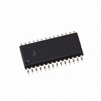
HI5731BIB Intersil, HI5731BIB Datasheet

HI5731BIB
Specifications of HI5731BIB
Available stocks
Related parts for HI5731BIB
HI5731BIB Summary of contents
Page 1
... HI5731BIPZ - PDIP (See Note) (Pb-free) HI5731BIB - SOIC HI5731BIB SOIC Tape and Reel HI5731BIBZ - SOIC (See Note) (Pb-free) HI5731-EVS 25 Evaluation Board (SOIC) NOTE: Intersil Pb-free products employ special Pb-free material sets; molding compounds/die attach materials and 100% matte tin plate termination finish, which is compatible with both SnPb and Pb-free soldering operations ...
Page 2
Typical Application Circuit 50Ω 0.1µF Functional Block Diagram (LSB 12-BIT D5 MASTER REGISTER D10 (MSB) D11 CLK AV AGND DV DGND HI5731 +5V HI5731 0.01µF DV (16) ...
Page 3
Absolute Maximum Ratings Digital Supply Voltage V to DGND . . . . . . . . . . . . . . . . . . . +5.5V CC Negative Digital Supply Voltage DV to DGND . . . ...
Page 4
Electrical Specifications PARAMETER Spurious Free Dynamic Range to Nyquist (Note 3) REFERENCE/CONTROL AMPLIFIER Internal Reference Voltage, V REF Internal Reference Voltage Drift Internal Reference Output Current Sink/Source Capability Internal Reference Load Regulation ...
Page 5
Timing Diagrams CLK D11-D0 I OUT t SETT t PD FIGURE 1. FULL SCALE SETTLING TIME DIAGRAM t CLK t SU D11-D0 I OUT t PD FIGURE 3. PROPAGATION DELAY, SETUP TIME, HOLD TIME AND MINIMUM PULSE WIDTH DIAGRAM 5 ...
Page 6
Typical Performance Curves 680 CLOCK FREQUENCY DOES NOT ALTER POWER DISSIPATION 640 600 560 -50 -30 - TEMPERATURE FIGURE 4. TYPICAL POWER DISSIPATION OVER TEMPERATURE 1.5 0.5 -0.5 1.5 0 600 1200 1800 2400 CODE FIGURE 6. TYPICAL ...
Page 7
Typical Performance Curves ATTEN 20dB RL -10.0dBm 10dB/ C CENTER 5.055MHz FIGURE 10. SPURIOUS FREE DYNAMIC RANGE = 76.16dBc ATTEN 20dB RL -10.0dBm 10dB CENTER 10.100MHz FIGURE 12. SPURIOUS FREE DYNAMIC RANGE = -81.67dBc ATTEN 20dB RL -10.0dBm ...
Page 8
Typical Performance Curves ATTEN 20dB RL -10.0dBm 10dB/ CENTER 10.133MHz FIGURE 16. SPURIOUS FREE DYNAMIC RANGE = 80.5dBc ATTEN 20dB RL -10.0dBm 10dB START FREQUENCY 500kHz STOP FREQUENCY 20MHz FIGURE 18. SPURIOUS FREE DYNAMIC RANGE = 71.16dBc S ...
Page 9
Pin Descriptions PIN NUMBER PIN NAME 1-12 D11 (MSB) thru Digital Data Bit 11, the Most Significant Bit thru Digital Data Bit 0, the Least Significant Bit. D0 (LSB) 15 CLK Data Clock Pin DC to 100MSPS. 13 ...
Page 10
HI5731 as possible on the analog (AV supplies. The analog and digital ground returns should be connected together back at the device to ensure proper operation on power up. The V power pin should also be CC decoupled with a ...
Page 11
... In order to minimize this, the Intersil HI5731 employes an internal register, just prior to the current sources, which is updated on the clock edge. Lastly, the worst case glitch on traditional D/A converters usually occurs at the major transition (i ...
Page 12
Interfacing to the HSP45106 NCO-16 The HSP45106 is a 16-bit, Numerically Controlled Oscillator (NCO). The HSP45106 can be used to generate various modulation schemes for Direct Digital Synthesis (DDS) applications. Figure 28 shows how to interface an HI5731 to the ...
Page 13
CLK BASEBAND BIT ENCODER STREAM V CC CONTROLLER FIGURE 28. MODULATOR USING THE HI5731 AND THE HSP45106 16-BIT NCO 13 HI5731 U2 K9 CLK C11 MOD2 B11 MOD1 C10 MOD0 A11 ...
Page 14
CLK I BASEBAND BIT ENCODER Q STREAM CONTROL BUS CONTROLLER FIGURE 29. PSK MODULATOR USING THE HI5731 AND THE HSP45102 12-BIT NCO 14 HI5731 CLK 6 1 OUT11 OUT10 20 ...
Page 15
Die Characteristics DIE DIMENSIONS 161.5 mils x 160.7 mils x 19 mils METALLIZATION Type: AlSiCu Å Å Thickness 17k Metallization Mask Layout HI5731 PASSIVATION ...
Page 16
Dual-In-Line Plastic Packages (PDIP INDEX N/2 AREA -B- -A- D BASE PLANE -C- SEATING PLANE 0.010 (0.25 NOTES: 1. Controlling Dimensions: INCH. In case of conflict between ...
Page 17
... Accordingly, the reader is cautioned to verify that data sheets are current before placing orders. Information furnished by Intersil is believed to be accurate and reliable. How- ever, no responsibility is assumed by Intersil or its subsidiaries for its use; nor for any infringements of patents or other rights of third parties which may result from its use. No license is granted by implication or otherwise under any patent or patent rights of Intersil or its subsidiaries ...


