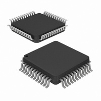
HI5828IN Intersil, HI5828IN Datasheet

HI5828IN
Specifications of HI5828IN
Available stocks
Related parts for HI5828IN
HI5828IN Summary of contents
Page 1
... HI5828’s segmented current source architecture. This device complements the HI5x60 and HI5x28 family of high speed converters, which includes 8, 10, 12, and 14-bit devices. Ordering Information TEMP. PART RANGE o NUMBER ( C) PACKAGE HI5828IN - LQFP HI5828EVAL2 25 Evaluation Platform Pinout HI5828 (LQFP) TOP VIEW ...
Page 2
Functional Block Diagram (LSB) QD0 QD1 QD2 QD3 QD4 QD5 MASTER QD6 LATCH QD7 QD8 QD9 QD10 (MSB) QD11 (LSB) ID0 ID1 ID2 ID3 ID4 MASTER ID5 ID6 LATCH ID7 ID8 ID9 ID10 (MSB) ID11 CLK DVDD DGND AVDD AGND ...
Page 3
Typical Applications Circuit ID5 ID4 ID3 ID2 ID1 ID0 (LSB) SLEEP DV PP ICOMP2 C 1 0.1µ 0.1µ 0.1µF +5V OR +3V POWER SOURCE NOTE: Separate analog and digital grounds should be used, in which case ...
Page 4
Pin Descriptions PIN NO. PIN NAME 11, 19, 26 AGND 13 VDD 28 CLK 27 DGND 10 D VDD 20 FSADJ 14, 23 ICOMP1, QCOMP1 12, 25 ICOMP2, QCOMP2 43-48, 1-6, ID11-ID0, QD11-QD0 Digital Data Input Ports. Bit ...
Page 5
Absolute Maximum Ratings Digital Supply Voltage D to DGND . . . . . . . . . . . . . . . . . . +5.5V VDD Analog Supply Voltage A to AGND . . . . . ...
Page 6
Electrical Specifications A VDD IOUTFS = 20mA, T PARAMETER Output Noise IOUTFS = 20mA IOUTFS = 2mA AC CHARACTERISTICS +5V Power Supply f CLK Spurious Free Dynamic Range, f CLK SFDR Within a Window f CLK +5V Power Supply f ...
Page 7
Electrical Specifications A VDD IOUTFS = 20mA, T PARAMETER +3V Power Supply f CLK Spurious Free Dynamic Range, f SFDR to Nyquist (f /2) CLK CLK f CLK f CLK f CLK f CLK f CLK f CLK f CLK ...
Page 8
Electrical Specifications A VDD IOUTFS = 20mA, T PARAMETER TIMING CHARACTERISTICS Data Setup Time, t See Figure 4 (Note 3) SU Data Hold Time, t See Figure 4 (Note 3) HLD Propagation Delay Time, t See Figure 4 PD CLK ...
Page 9
Definition of Specifications Differential Linearity Error, DNL, is the measure of the step size output deviation from code to code. Ideally the step size should be 1 LSB. A DNL specification of 1 LSB or less guarantees monotonicity. Full Scale ...
Page 10
Ground Planes Separate digital and analog ground planes should be used. All of the digital functions of the device and their corresponding components should be located over the digital ground plane and terminated to the digital ground plane. The same ...
Page 11
Timing Diagrams CLK D11-D0 I OUT t SETT t PD FIGURE 2. OUTPUT SETTLING TIME DIAGRAM CLK t SU D11-D0 I OUT t PD FIGURE 4. PROPAGATION DELAY, SETUP TIME, HOLD TIME AND MINIMUM PULSE WIDTH DIAGRAM 11 HI5828 50% ...
Page 12
... Accordingly, the reader is cautioned to verify that data sheets are current before placing orders. Information furnished by Intersil is believed to be accurate and reliable. How- ever, no responsibility is assumed by Intersil or its subsidiaries for its use; nor for any infringements of patents or other rights of third parties which may result from its use. No license is granted by implication or otherwise under any patent or patent rights of Intersil or its subsidiaries ...


