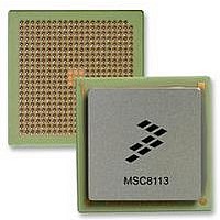
MSC8113TVT3600V Freescale Semiconductor, MSC8113TVT3600V Datasheet - Page 39

MSC8113TVT3600V
Manufacturer Part Number
MSC8113TVT3600V
Description
DSP TRI-CORE 431-FCPBGA
Manufacturer
Freescale Semiconductor
Series
MSC81xx StarCorer
Type
SC140 Corer
Datasheet
1.MSC8113TMP3600V.pdf
(44 pages)
Specifications of MSC8113TVT3600V
Interface
Ethernet, I²C, TDM, UART
Clock Rate
300MHz
Non-volatile Memory
External
On-chip Ram
1.436MB
Voltage - I/o
3.30V
Voltage - Core
1.10V
Operating Temperature
-40°C ~ 105°C
Mounting Type
Surface Mount
Package / Case
431-FCPBGA
Svhc
No SVHC (15-Dec-2010)
Base Number
8113
Cache On Chip L1/l2 Memory
64KB
Core Frequency Typ
300MHz
Dsp Type
Tri Core
External Supported Memory
SRAM, SDRAM
Interface Type
TDM, I2C, UART,
Rohs Compliant
Yes
Lead Free Status / RoHS Status
Lead free / RoHS Compliant
Available stocks
Company
Part Number
Manufacturer
Quantity
Price
Company:
Part Number:
MSC8113TVT3600V
Manufacturer:
Freescale Semiconductor
Quantity:
10 000
Each
GND
chip. The
four sides of the package. The capacitor leads and associated printed circuit traces connecting to chip
be kept to less than half an inch per capacitor lead. A four-layer board is recommended, employing two inner layers as
GND
All output pins on the MSC8113 have fast rise and fall times. PCB trace interconnection length should be minimized to
minimize undershoot and reflections caused by these fast output switching times. This recommendation particularly applies to
the address and data buses. Maximum PCB trace lengths of six inches are recommended. For the DSI control signals in
synchronous mode, ensure that the layout supports the DSI AC timing requirements and minimizes any signal crosstalk.
Capacitance calculations should consider all device loads as well as parasitic capacitances due to the PCB traces. Attention to
proper PCB layout and bypassing becomes especially critical in systems with higher capacitive loads because these loads create
higher transient currents in the
Special care should be taken to minimize the noise levels on the PLL supply pins. There is one pair of PLL supply pins:
V
Figure 34. For optimal noise filtering, place the circuit as close as possible to
to
kept short and direct. Provide an extremely low impedance path to the ground plane for
by a 0.01-µF capacitor located as close as possible to the chip package. For best results, place this capacitor on the backside of
the PCB aligned with the depopulated void on the MSC8113 located in the square defined by positions, L11, L12, L13, M11,
M12, M13, N11, N12, and N13.
3.3
Unused output pins can be disconnected, and unused input pins should be connected to the non-active value, via resistors to
V
Freescale Semiconductor
CCSYN
DDH
V
CCSYN
•
•
•
•
•
•
•
•
V
pin should have a low-impedance path to the ground plane. The power supply pins drive distinct groups of logic on the
planes.
or
CC
-
GND
GND
If the DSI is unused (DDR[DSIDIS] is set),
disconnected.
When the DSI uses synchronous mode,
up or down, depending on design requirements.
HDST
DCR[DSRFA] bit is set.
When the DSI is in 64-bit data bus mode and DCR[BEM] is cleared, pull up
HDBE[1–3]
When the DSI is in 32-bit data bus mode and DCR[BEM] is cleared,
must be pulled up.
When the DSI is in asynchronous mode,
The following signals must be pulled up:
In single-master mode (BCR[EBM] = 0) with internal arbitration (PPC_ACR[EARB] = 0):
—
—
—
—
V
and
, followed by the 10-µF capacitor, the 10-nH inductor, and finally the 10-Ω resistor to
CC
Connectivity Guidelines
BG
EXT_BG[2–3]
functionality. For any other functionality, connect the signal lines based on the multiplexed functionality.
BR
EXT_BR[2–3]
SYN
, except for the following:
V
power supply should have at least four 0.1 µF by-pass capacitors to ground located as closely as possible to the
can be disconnected if the DSI is in big-endian mode, or if the DSI is in little-endian mode and the
DD
,
. To ensure internal clock stability, filter the power to the
must be pulled up.
DBG
pin on the MSC8113 device should have a low-impedance path to the board power supply. Similarly, each
and
, and
HWBS[4–7]
,
TS
must be pulled up if multiplexed to the system bus functionality.
EXT_DBG[2–3]
MSC8113 Tri-Core Digital Signal Processor Data Sheet, Rev. 1
V
can be left unconnected.
CC
V
,
DD
V
/
DD
HDBS[4–7]
, and
10Ω
, and
GND
Figure 34. V
/
HTA
HWBE[4–7]
GBL
HBRST
10nH
HRESET
circuits. Pull up all unused inputs or signals that will be inputs during reset.
HCS
must be pulled up. In asynchronous mode,
can be left unconnected if they are multiplexed to the system bus
10 µF
and
and
,
SRESET
/
CCSYN
HDBE[4–7]
HCLKIN
HBCS
Bypass
,
must pulled up and all the rest of the DSI signals can be
ARTRY
should either be disconnected or pulled up.
/
PWE[4–7]
V
CCSYN
V
HWBS[1–3]
,
CCSYN
TA
0.01 µF
,
input with a circuit similar to the one in
TEA
V
/
. The 0.01-µF capacitor should be closest
PSDDQM[4–7]
CCSYN
HWBS[1–3]
,
GND
PSDVAL
/
HDBS[1–3]
Hardware Design Considerations
SYN
V
. Bypass
HTA
/
, and
DD
HDBS[1–3]
V
/
PBS[4–7]
CC
. These traces should be
/
should be pulled either
HWBE[1–3]
AACK
,
V
DD
GND
, and
.
/
.
HWBE[1–3]
SYN
GND
/
HDBE[1–3]
to
V
V
CC
should
CCSYN
and
/
39


