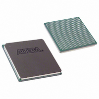
EP1S20F780C7N Altera, EP1S20F780C7N Datasheet - Page 193

EP1S20F780C7N
Manufacturer Part Number
EP1S20F780C7N
Description
IC STRATIX FPGA 20K LE 780-FBGA
Manufacturer
Altera
Series
Stratix®r
Datasheet
1.EP1S10F780C7.pdf
(276 pages)
Specifications of EP1S20F780C7N
Number Of Logic Elements/cells
18460
Number Of Labs/clbs
1846
Total Ram Bits
1669248
Number Of I /o
586
Voltage - Supply
1.425 V ~ 1.575 V
Mounting Type
Surface Mount
Operating Temperature
0°C ~ 85°C
Package / Case
780-FBGA
Family Name
Stratix
Number Of Logic Blocks/elements
18460
# I/os (max)
586
Frequency (max)
420.17MHz
Process Technology
0.13um (CMOS)
Operating Supply Voltage (typ)
1.5V
Logic Cells
18460
Ram Bits
1669248
Operating Supply Voltage (min)
1.425V
Operating Supply Voltage (max)
1.575V
Operating Temp Range
0C to 85C
Operating Temperature Classification
Commercial
Mounting
Surface Mount
Pin Count
780
Package Type
FC-FBGA
Lead Free Status / RoHS Status
Lead free / RoHS Compliant
Number Of Gates
-
Lead Free Status / Rohs Status
Compliant
Other names
544-1855
EP1S20F780C7N
EP1S20F780C7N
Available stocks
Company
Part Number
Manufacturer
Quantity
Price
Company:
Part Number:
EP1S20F780C7N
Manufacturer:
ALTERA
Quantity:
3 000
- Current page: 193 of 276
- Download datasheet (4Mb)
Altera Corporation
January 2006
t
t
t
t
t
t
t
t
t
t
t
t
SU
H
CO
INREG2PIPE9
INREG2PIPE18
PIPE2OUTREG2ADD
PIPE2OUTREG4ADD
PD9
PD18
PD36
CLR
CLKHL
Table 4–39. DSP Block Internal Timing Microparameter Descriptions
Symbol
Input, pipeline, and output register setup time before clock
Input, pipeline, and output register hold time after clock
Input, pipeline, and output register clock-to-output delay
Input Register to DSP Block pipeline register in 9 × 9-bit
mode
Input Register to DSP Block pipeline register in 18 × 18-bit
mode
DSP Block Pipeline Register to output register delay in Two-
Multipliers Adder mode
DSP Block Pipeline Register to output register delay in Four-
Multipliers Adder mode
Combinatorial input to output delay for 9 × 9
Combinatorial input to output delay for 18 × 18
Combinatorial input to output delay for 36 × 36
Minimum clear pulse width
Register minimum clock high or low time. This is a limit on
the min time for the clock on the registers in these blocks.
The actual performance is dependent upon the internal
point-to-point delays in the blocks and may give slower
performance as shown in
reported by the timing analyzer in the Quartus II software.
Stratix Device Handbook, Volume 1
Parameter
Table 4–36 on page 4–20
DC & Switching Characteristics
and as
4–23
Related parts for EP1S20F780C7N
Image
Part Number
Description
Manufacturer
Datasheet
Request
R

Part Number:
Description:
CYCLONE II STARTER KIT EP2C20N
Manufacturer:
Altera
Datasheet:

Part Number:
Description:
CPLD, EP610 Family, ECMOS Process, 300 Gates, 16 Macro Cells, 16 Reg., 16 User I/Os, 5V Supply, 35 Speed Grade, 24DIP
Manufacturer:
Altera Corporation
Datasheet:

Part Number:
Description:
CPLD, EP610 Family, ECMOS Process, 300 Gates, 16 Macro Cells, 16 Reg., 16 User I/Os, 5V Supply, 15 Speed Grade, 24DIP
Manufacturer:
Altera Corporation
Datasheet:

Part Number:
Description:
Manufacturer:
Altera Corporation
Datasheet:

Part Number:
Description:
CPLD, EP610 Family, ECMOS Process, 300 Gates, 16 Macro Cells, 16 Reg., 16 User I/Os, 5V Supply, 30 Speed Grade, 24DIP
Manufacturer:
Altera Corporation
Datasheet:

Part Number:
Description:
High-performance, low-power erasable programmable logic devices with 8 macrocells, 10ns
Manufacturer:
Altera Corporation
Datasheet:

Part Number:
Description:
High-performance, low-power erasable programmable logic devices with 8 macrocells, 7ns
Manufacturer:
Altera Corporation
Datasheet:

Part Number:
Description:
Classic EPLD
Manufacturer:
Altera Corporation
Datasheet:

Part Number:
Description:
High-performance, low-power erasable programmable logic devices with 8 macrocells, 10ns
Manufacturer:
Altera Corporation
Datasheet:

Part Number:
Description:
Manufacturer:
Altera Corporation
Datasheet:

Part Number:
Description:
Manufacturer:
Altera Corporation
Datasheet:

Part Number:
Description:
Manufacturer:
Altera Corporation
Datasheet:

Part Number:
Description:
CPLD, EP610 Family, ECMOS Process, 300 Gates, 16 Macro Cells, 16 Reg., 16 User I/Os, 5V Supply, 25 Speed Grade, 24DIP
Manufacturer:
Altera Corporation
Datasheet:


