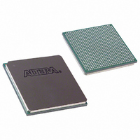
EP1S20F780C7N Altera, EP1S20F780C7N Datasheet - Page 230

EP1S20F780C7N
Manufacturer Part Number
EP1S20F780C7N
Description
IC STRATIX FPGA 20K LE 780-FBGA
Manufacturer
Altera
Series
Stratix®r
Datasheet
1.EP1S10F780C7.pdf
(276 pages)
Specifications of EP1S20F780C7N
Number Of Logic Elements/cells
18460
Number Of Labs/clbs
1846
Total Ram Bits
1669248
Number Of I /o
586
Voltage - Supply
1.425 V ~ 1.575 V
Mounting Type
Surface Mount
Operating Temperature
0°C ~ 85°C
Package / Case
780-FBGA
Family Name
Stratix
Number Of Logic Blocks/elements
18460
# I/os (max)
586
Frequency (max)
420.17MHz
Process Technology
0.13um (CMOS)
Operating Supply Voltage (typ)
1.5V
Logic Cells
18460
Ram Bits
1669248
Operating Supply Voltage (min)
1.425V
Operating Supply Voltage (max)
1.575V
Operating Temp Range
0C to 85C
Operating Temperature Classification
Commercial
Mounting
Surface Mount
Pin Count
780
Package Type
FC-FBGA
Lead Free Status / RoHS Status
Lead free / RoHS Compliant
Number Of Gates
-
Lead Free Status / Rohs Status
Compliant
Other names
544-1855
EP1S20F780C7N
EP1S20F780C7N
Available stocks
Company
Part Number
Manufacturer
Quantity
Price
Company:
Part Number:
EP1S20F780C7N
Manufacturer:
ALTERA
Quantity:
3 000
- Current page: 230 of 276
- Download datasheet (4Mb)
Timing Model
4–60
Stratix Device Handbook, Volume 1
Skew on Input Pins
Table 4–99
worst case I/O skew value. You can use these values, for example, when
calculating the timing budget on the input (read) side of a memory
interface.
PLL Counter & Clock Network Skews
Table 4–100
the Stratix device PLL.
I/O Timing Measurement Methodology
Different I/O standards require different baseline loading techniques for
reporting timing delays. Altera characterizes timing delays with the
required termination and loading for each I/O standard. The timing
information is specified from the input clock pin up to the output pin of
Note to
(1)
Pins in the same I/O bank
Pins in top/bottom (vertical I/O) banks
Pins in left/right side (horizontal I/O) banks
Pins across the entire device
Clock skew between two external clock outputs driven
by the same counter
Clock skew between two external clock outputs driven
by the different counters with the same settings
Dual-purpose PLL dedicated clock output used as I/O
pin vs. regular I/O pin
Clock skew between any two outputs of the PLL that
drive global clock networks
Table 4–99. Package Skew on Input Pins
Table 4–100. PLL Counter & Clock Network Skews
The Quartus II software models 270 ps of delay on the PLL dedicated clock
output (PLL6_OUT[3..0]p/n and PLL5_OUT[3..0]p/n) pins both when
used as clocks and when used as I/O pins.
Table
shows the package skews that were considered to get the
shows the clock skews between different clock outputs from
4–100:
Package Parameter
Parameter
Worst-Case Skew (ps)
Worst-Case Skew (ps)
Altera Corporation
270
100
50
50
50
100
150
150
January 2006
(1)
Related parts for EP1S20F780C7N
Image
Part Number
Description
Manufacturer
Datasheet
Request
R

Part Number:
Description:
CYCLONE II STARTER KIT EP2C20N
Manufacturer:
Altera
Datasheet:

Part Number:
Description:
CPLD, EP610 Family, ECMOS Process, 300 Gates, 16 Macro Cells, 16 Reg., 16 User I/Os, 5V Supply, 35 Speed Grade, 24DIP
Manufacturer:
Altera Corporation
Datasheet:

Part Number:
Description:
CPLD, EP610 Family, ECMOS Process, 300 Gates, 16 Macro Cells, 16 Reg., 16 User I/Os, 5V Supply, 15 Speed Grade, 24DIP
Manufacturer:
Altera Corporation
Datasheet:

Part Number:
Description:
Manufacturer:
Altera Corporation
Datasheet:

Part Number:
Description:
CPLD, EP610 Family, ECMOS Process, 300 Gates, 16 Macro Cells, 16 Reg., 16 User I/Os, 5V Supply, 30 Speed Grade, 24DIP
Manufacturer:
Altera Corporation
Datasheet:

Part Number:
Description:
High-performance, low-power erasable programmable logic devices with 8 macrocells, 10ns
Manufacturer:
Altera Corporation
Datasheet:

Part Number:
Description:
High-performance, low-power erasable programmable logic devices with 8 macrocells, 7ns
Manufacturer:
Altera Corporation
Datasheet:

Part Number:
Description:
Classic EPLD
Manufacturer:
Altera Corporation
Datasheet:

Part Number:
Description:
High-performance, low-power erasable programmable logic devices with 8 macrocells, 10ns
Manufacturer:
Altera Corporation
Datasheet:

Part Number:
Description:
Manufacturer:
Altera Corporation
Datasheet:

Part Number:
Description:
Manufacturer:
Altera Corporation
Datasheet:

Part Number:
Description:
Manufacturer:
Altera Corporation
Datasheet:

Part Number:
Description:
CPLD, EP610 Family, ECMOS Process, 300 Gates, 16 Macro Cells, 16 Reg., 16 User I/Os, 5V Supply, 25 Speed Grade, 24DIP
Manufacturer:
Altera Corporation
Datasheet:


