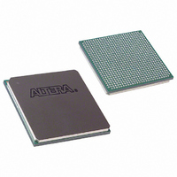
EP3C120F780C8 Altera, EP3C120F780C8 Datasheet - Page 13

EP3C120F780C8
Manufacturer Part Number
EP3C120F780C8
Description
IC CYCLONE III FPGA 119K 780FBGA
Manufacturer
Altera
Series
Cyclone® IIIr
Datasheets
1.EP3C5F256C8N.pdf
(5 pages)
2.EP3C5F256C8N.pdf
(34 pages)
3.EP3C5F256C8N.pdf
(66 pages)
4.EP3C5F256C8N.pdf
(14 pages)
5.EP3C5F256C8N.pdf
(76 pages)
Specifications of EP3C120F780C8
Number Of Logic Elements/cells
119088
Number Of Labs/clbs
7443
Total Ram Bits
3981312
Number Of I /o
531
Voltage - Supply
1.15 V ~ 1.25 V
Mounting Type
Surface Mount
Operating Temperature
0°C ~ 85°C
Package / Case
780-FBGA
For Use With
544-2601 - KIT DEV CYCLONE III LS EP3CLS200544-2589 - KIT DEV EMB CYCLONE III EDITION544-2566 - KIT DEV DSP CYCLONE III EDITION544-2444 - KIT DEV CYCLONE III EP3C120544-2411 - KIT DEV NIOS II CYCLONE III ED.
Lead Free Status / RoHS Status
Contains lead / RoHS non-compliant
Number Of Gates
-
Other names
544-2391
544-2531
544-2531
EP3C120F780C8ES
544-2531
544-2531
EP3C120F780C8ES
Available stocks
Company
Part Number
Manufacturer
Quantity
Price
Company:
Part Number:
EP3C120F780C8
Manufacturer:
ALTERA
Quantity:
561
Company:
Part Number:
EP3C120F780C8N
Manufacturer:
ALTERA
Quantity:
642
Part Number:
EP3C120F780C8N
Manufacturer:
ALTERA/阿尔特拉
Quantity:
20 000
Early System Planning
© November 2008 Altera Corporation
f
f
1
1
To know whether the input frequencies and output frequencies can be implemented
in one PLL, enter your settings when instantiating the altpll megafunction through
the Quartus II software.
To obtain the input and output clock frequency range specifications for the different
device speed grades, refer to the
Characteristics
Number of Clock Inputs
Cyclone III PLLs can have a maximum of two clock inputs, where only one clock
input functions at a time. You need two clock inputs for your PLL for applications
such as clock redundancy or dual clock domain. Clock redundancy application
ensures there is a back-up input clock in case the current clock is not present. A dual
clock application enables the PLL to change to another input clock frequency during
operation. This feature is called clock switchover.
Cyclone III devices have automatic and manual clock switchover. Automatic
switchover enables the PLL to change to another clock input after the current clock
input becomes unavailable. Manual clock switchover enables the user to control the
switch of the input clocks.
If you do not use the PLL for these applications, one clock input is sufficient.
You can enable the clock switchover feature from the altpll megafunction.
Number of Clock Outputs
Cyclone III PLLs can have a maximum of five clock outputs (c0-c4). You can connect
the c0 clock output to the dedicated external clock output pin (recommended as this
minimizes the clock jitter), normal user I/O or dedicated global clock network. The
c1, c2, c3, and c4 clock outputs can be connected to the user I/O pins or dedicated
global clock networks.
Clock Input and Output I/O Standard
Dedicated clock input pins can support all I/O standards supported by the
Cyclone III device, except PPDS, RSDS, and mini-LVDS. Dedicated external clock
output pins can support all I/O standards supported by the Cyclone III device.
For more information about the I/O standard support, refer to the
I/O Features
PLL Design
After defining the requirements, these are the items that you must consider while
designing the PLL according to your application.
Selecting the Right Compensation Mode
Table 5
shows the four compensation modes that Cyclone III devices support.
chapter in volume 1 of the Cyclone III Device Handbook.
chapter in volume 2 of the Cyclone III Device Handbook
Cyclone III Device Datasheet: DC and Switching
Cyclone III Device
Page 13


