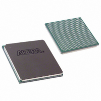
EP3C120F780C8 Altera, EP3C120F780C8 Datasheet - Page 18

EP3C120F780C8
Manufacturer Part Number
EP3C120F780C8
Description
IC CYCLONE III FPGA 119K 780FBGA
Manufacturer
Altera
Series
Cyclone® IIIr
Datasheets
1.EP3C5F256C8N.pdf
(5 pages)
2.EP3C5F256C8N.pdf
(34 pages)
3.EP3C5F256C8N.pdf
(66 pages)
4.EP3C5F256C8N.pdf
(14 pages)
5.EP3C5F256C8N.pdf
(76 pages)
Specifications of EP3C120F780C8
Number Of Logic Elements/cells
119088
Number Of Labs/clbs
7443
Total Ram Bits
3981312
Number Of I /o
531
Voltage - Supply
1.15 V ~ 1.25 V
Mounting Type
Surface Mount
Operating Temperature
0°C ~ 85°C
Package / Case
780-FBGA
For Use With
544-2601 - KIT DEV CYCLONE III LS EP3CLS200544-2589 - KIT DEV EMB CYCLONE III EDITION544-2566 - KIT DEV DSP CYCLONE III EDITION544-2444 - KIT DEV CYCLONE III EP3C120544-2411 - KIT DEV NIOS II CYCLONE III ED.
Lead Free Status / RoHS Status
Contains lead / RoHS non-compliant
Number Of Gates
-
Other names
544-2391
544-2531
544-2531
EP3C120F780C8ES
544-2531
544-2531
EP3C120F780C8ES
Available stocks
Company
Part Number
Manufacturer
Quantity
Price
Company:
Part Number:
EP3C120F780C8
Manufacturer:
ALTERA
Quantity:
561
Company:
Part Number:
EP3C120F780C8N
Manufacturer:
ALTERA
Quantity:
642
Part Number:
EP3C120F780C8N
Manufacturer:
ALTERA/阿尔特拉
Quantity:
20 000
Page 18
f
f
f
For details about implementing these features, refer to the
volume 2 of the Quartus II Handbook.
Minimizing Simultaneous Switching Noise
Simultaneous switching noise (SSN) becomes a concern when too many pins within
close proximity change levels at the same time and cause V
on the quiet pins nearby. Noise generated by SSN can reduce noise margin and cause
incorrect switching.
When creating your design, try to separate the pins that switch simultaneously. If
possible, distribute the switching pins to different I/O banks. Set the unused I/O pins
nearby to V
also turn on the slow slew rate feature and use a lower drive strength for the
switching pins. Proper termination on the switching I/O pins also helps to reduce
reflection and the SSN effect on the quiet pins.
For details about the sources of the SSN, ways to mitigate SSN and guidelines on a
PCB design for the general high speed digital designs, refer to
Simultaneous Switching Noise (SSN) Design Guidelines.
For board design guidelines, refer to
AN 315: Guidelines for Designing High-Speed FPGA PCBs.
Unused Pin Connection
The Quartus II software generates the pin report file (.pin) when you compile your
design. This report file specifies how you should connect the unused pins of your
device. For a Cyclone III device, unused I/O pins are marked in the report file as any
one of the following depending on how you set the unused pins in the Quartus II
software:
■
■
■
■
■
All I/O pins specified as GND* can either be connected to ground to improve the
device's immunity to noise, or left unconnected. Leave all RESERVE I/O pins
unconnected on your board because these I/O pins drive out unspecified signals.
Tying a RESERVED I/O pin to V
contention that can damage the output driver of the device.
RESERVED_INPUT I/O pins can be connected to a high or low signal on the board
while RESERVED_INPUT_WITH_WEAK_PULLUP and
RESERVED_INPUT_WITH_BUS_HOLD pins can be left unconnected.
GND*
RESERVED
RESERVED_INPUT
RESERVED_INPUT_WITH_WEAK_PULLUP
RESERVED_INPUT_WITH_BUS_HOLD
CC
to minimize V
CC
sag, or to ground to minimize ground bounce. You can
CC
, ground, or another signal source can create
AN 224: High-Speed Board Layout Guidelines
© November 2008 Altera Corporation
I/O Management
CC
sag or ground bounce
AN 508: Cyclone III
Board Design Considerations
chapter in
and


