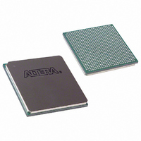
EP3C120F780C8 Altera, EP3C120F780C8 Datasheet - Page 39

EP3C120F780C8
Manufacturer Part Number
EP3C120F780C8
Description
IC CYCLONE III FPGA 119K 780FBGA
Manufacturer
Altera
Series
Cyclone® IIIr
Datasheets
1.EP3C5F256C8N.pdf
(5 pages)
2.EP3C5F256C8N.pdf
(34 pages)
3.EP3C5F256C8N.pdf
(66 pages)
4.EP3C5F256C8N.pdf
(14 pages)
5.EP3C5F256C8N.pdf
(76 pages)
Specifications of EP3C120F780C8
Number Of Logic Elements/cells
119088
Number Of Labs/clbs
7443
Total Ram Bits
3981312
Number Of I /o
531
Voltage - Supply
1.15 V ~ 1.25 V
Mounting Type
Surface Mount
Operating Temperature
0°C ~ 85°C
Package / Case
780-FBGA
For Use With
544-2601 - KIT DEV CYCLONE III LS EP3CLS200544-2589 - KIT DEV EMB CYCLONE III EDITION544-2566 - KIT DEV DSP CYCLONE III EDITION544-2444 - KIT DEV CYCLONE III EP3C120544-2411 - KIT DEV NIOS II CYCLONE III ED.
Lead Free Status / RoHS Status
Contains lead / RoHS non-compliant
Number Of Gates
-
Other names
544-2391
544-2531
544-2531
EP3C120F780C8ES
544-2531
544-2531
EP3C120F780C8ES
Available stocks
Company
Part Number
Manufacturer
Quantity
Price
Company:
Part Number:
EP3C120F780C8
Manufacturer:
ALTERA
Quantity:
561
Company:
Part Number:
EP3C120F780C8N
Manufacturer:
ALTERA
Quantity:
642
Part Number:
EP3C120F780C8N
Manufacturer:
ALTERA/阿尔特拉
Quantity:
20 000
Design and Compilation
I/O Considerations
© November 2008 Altera Corporation
f
Architectural Optimization
Use specific device architecture features to reduce power consumption. For example,
use the dedicated DSP block available in the Cyclone III device in place of LEs to
perform arithmetic-related functions; build large shift registers from RAM-based
FIFO buffers instead of building the shift registers from the LE registers.
Cyclone III devices offer increased system integration with enhancements in I/O
flexibility and improvements in features. I/O capabilities of the FPGA device, board
layout guidelines, and signal integrity concerns significantly influence pin location
decisions and other types of assignments for each of your design pins. You can
optimize I/O resources for performance and cost while avoiding undesirable signal
issues with the tools and taking into account considerations described in this section.
I/O Tools
I/O design flow includes creating pin-related assignments and validating them
against pin placement guidelines. Use the Pin Planner and Assignment Editor tools in
the Quartus II software to help you through the pin-related assignment creation and
editing. I/O Assignment Analysis helps you to check the legality of the pin
assignments. The following subsections discuss the tools used to create and edit
pin-related assignments.
Pin Planner
The Pin Planner is used to create and edit pin-related assignments. Use the Pin
Planner Package View to make pin location and other assignments using a device
package view instead of pin numbers. With the Pin Planner, you can visually identify
I/O banks, V
pins in the Package View helps you to minimize signal breakout congestion on board
layout when making pin location assignments.
Complementing the Pin Planner is the Pad View window, which displays the pads in
the order around the silicon die. Package pins are connected to pads located on the
perimeter of the top metal layer of the silicon die. Note the pad location where your
pins were assigned, because some pin placement rules describe pad placement
restrictions. Use the Pad View window to guide your pin placement decisions to
maintain good signal integrity for the interface in your design.
The Pin Migration View in the Pin Planner tool shows the pins that will change
function in a migration device if you select one or more migration devices for your
project. It helps you to identify the differences in pins which can exist between
migration devices.
For details about using the Package View, Pad View, and Pin Migration View in the
Pin Planner tool, refer to the Using the Pin Planner section of the
chapter in volume 2 of the Quartus II Handbook.
Assignment Editor
While the Pin Planner provides an intuitive graphical representation of the targeted
device, the Assignment Editor provides a spreadsheet-like interface that allows you to
create and change all pin-related assignments.
REF
groups, and differential pin pairings. The visual representation of
I/O Management
Page 39


