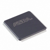
EPF10K20TC144-4N Altera, EPF10K20TC144-4N Datasheet - Page 120

EPF10K20TC144-4N
Manufacturer Part Number
EPF10K20TC144-4N
Description
IC FLEX 10K FPGA 20K 144-TQFP
Manufacturer
Altera
Series
FLEX-10K®r
Datasheet
1.EPF10K10ATC100-3.pdf
(128 pages)
Specifications of EPF10K20TC144-4N
Number Of Logic Elements/cells
1152
Number Of Labs/clbs
144
Total Ram Bits
12288
Number Of I /o
102
Number Of Gates
63000
Voltage - Supply
4.75 V ~ 5.25 V
Mounting Type
Surface Mount
Operating Temperature
0°C ~ 85°C
Package / Case
144-TQFP, 144-VQFP
Family Name
FLEX 10K
Number Of Usable Gates
20000
Number Of Logic Blocks/elements
1152
# I/os (max)
102
Frequency (max)
125MHz
Process Technology
CMOS
Operating Supply Voltage (typ)
5V
Logic Cells
1152
Ram Bits
12288
Device System Gates
63000
Operating Supply Voltage (min)
4.75V
Operating Supply Voltage (max)
5.25V
Operating Temp Range
0C to 70C
Operating Temperature Classification
Commercial
Mounting
Surface Mount
Pin Count
144
Package Type
TQFP
Lead Free Status / RoHS Status
Lead free / RoHS Compliant
Other names
544-2219
Available stocks
Company
Part Number
Manufacturer
Quantity
Price
Company:
Part Number:
EPF10K20TC144-4N
Manufacturer:
Altera
Quantity:
135
Company:
Part Number:
EPF10K20TC144-4N
Manufacturer:
ALTERA31
Quantity:
2 640
Part Number:
EPF10K20TC144-4N
Manufacturer:
ALTERA
Quantity:
20 000
Notes:
(1)
(2)
(3)
Power
Consumption
120
FLEX 10K Embedded Programmable Logic Device Family Data Sheet
f
f
t
t
t
t
Symbol
CLKDEV1
CLKDEV2
INCLKSTB
LOCK
JITTER
OUTDUTY
Table 113. ClockLock & ClockBoost Parameters
To implement the ClockLock and ClockBoost circuitry with the MAX+PLUS II software, designers must specify the
input frequency. The MAX+PLUS II software tunes the PLL in the ClockLock and ClockBoost circuitry to this
frequency. The f
during device operation. Simulation does not reflect this parameter.
During device configuration, the ClockLock and ClockBoost circuitry is configured before the rest of the device. If
the incoming clock is supplied during configuration, the ClockLock and ClockBoost circuitry locks during
configuration, because the t
The t
JITTER
Input deviation from user specification in MAX+PLUS II (ClockBoost clock
multiplication factor equals 1)
Input deviation from user specification in MAX+PLUS II (ClockBoost clock
multiplication factor equals 2)
Input clock stability (measured between adjacent clocks)
Time required for ClockLock or ClockBoost to acquire lock
Jitter on ClockLock or ClockBoost-generated clock
Duty cycle for ClockLock or ClockBoost-generated clock
specification is measured under long-term observation.
CLKDEV
parameter specifies how much the incoming clock can differ from the specified frequency
The supply power (P) for FLEX 10K devices can be calculated with the
following equation:
P = P
Typical I
operating conditions tables on pages 46, 49, and 52 of this data sheet. The
I
logic. This value is calculated based on the amount of current that each LE
typically consumes. The P
load characteristics and switching frequency, can be calculated using the
guidelines given in Application Note 74 (Evaluating Power for Altera Devices).
1
The I
The parameters in this equation are shown below:
I
CCACTIVE
LOCK
CCACTIVE
CCACTIVE
value is less than the time required for configuration.
INT
(1)
(1)
CCSTANDBY
+ P
Compared to the rest of the device, the embedded array
consumes a negligible amount of power. Therefore, the
embedded array can be ignored when calculating supply
current.
Parameter
value depends on the switching frequency and the application
= K f
IO
= (I
value is calculated with the following equation:
MAX
CCSTANDBY
values are shown as I
(Part 2 of 2)
(3)
N tog
IO
(2)
value, which depends on the device output
+ I
LC
CCACTIVE )
-------------------------- -
MHz LE
CC0
A
V
in the FLEX 10K device DC
CC
Min
40
+ P
IO
Typ
50
Altera Corporation
Max
100
10
60
0.5
1
1
Unit
MHz
MHz
ps
ns
%
s


