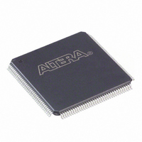
EPF10K20TC144-4N Altera, EPF10K20TC144-4N Datasheet - Page 31

EPF10K20TC144-4N
Manufacturer Part Number
EPF10K20TC144-4N
Description
IC FLEX 10K FPGA 20K 144-TQFP
Manufacturer
Altera
Series
FLEX-10K®r
Datasheet
1.EPF10K10ATC100-3.pdf
(128 pages)
Specifications of EPF10K20TC144-4N
Number Of Logic Elements/cells
1152
Number Of Labs/clbs
144
Total Ram Bits
12288
Number Of I /o
102
Number Of Gates
63000
Voltage - Supply
4.75 V ~ 5.25 V
Mounting Type
Surface Mount
Operating Temperature
0°C ~ 85°C
Package / Case
144-TQFP, 144-VQFP
Family Name
FLEX 10K
Number Of Usable Gates
20000
Number Of Logic Blocks/elements
1152
# I/os (max)
102
Frequency (max)
125MHz
Process Technology
CMOS
Operating Supply Voltage (typ)
5V
Logic Cells
1152
Ram Bits
12288
Device System Gates
63000
Operating Supply Voltage (min)
4.75V
Operating Supply Voltage (max)
5.25V
Operating Temp Range
0C to 70C
Operating Temperature Classification
Commercial
Mounting
Surface Mount
Pin Count
144
Package Type
TQFP
Lead Free Status / RoHS Status
Lead free / RoHS Compliant
Other names
544-2219
Available stocks
Company
Part Number
Manufacturer
Quantity
Price
Company:
Part Number:
EPF10K20TC144-4N
Manufacturer:
Altera
Quantity:
135
Company:
Part Number:
EPF10K20TC144-4N
Manufacturer:
ALTERA31
Quantity:
2 640
Part Number:
EPF10K20TC144-4N
Manufacturer:
ALTERA
Quantity:
20 000
Altera Corporation
Each IOE selects the clock, clear, clock enable, and output enable controls
from a network of I/O control signals called the peripheral control bus.
The peripheral control bus uses high-speed drivers to minimize signal
skew across devices; it provides up to 12 peripheral control signals that
can be allocated as follows:
If more than six clock enable or eight output enable signals are required,
each IOE on the device can be controlled by clock enable and output
enable signals driven by specific LEs. In addition to the two clock signals
available on the peripheral control bus, each IOE can use one of two
dedicated clock pins. Each peripheral control signal can be driven by any
of the dedicated input pins or the first LE of each LAB in a particular row.
In addition, an LE in a different row can drive a column interconnect,
which causes a row interconnect to drive the peripheral control signal.
The chip-wide reset signal will reset all IOE registers, overriding any other
control signals.
Tables 8
rows that can drive global signals. These tables also show how the output
enable, clock enable, clock, and clear signals share 12 peripheral control
signals.
Up to eight output enable signals
Up to six clock enable signals
Up to two clock signals
Up to two clear signals
FLEX 10K Embedded Programmable Logic Device Family Data Sheet
and
9
list the sources for each peripheral control signal, and the
31


