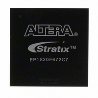
EP1S20F672C7 Altera, EP1S20F672C7 Datasheet - Page 10

EP1S20F672C7
Manufacturer Part Number
EP1S20F672C7
Description
IC STRATIX FPGA 20K LE 672-FBGA
Manufacturer
Altera
Series
Stratix®r
Datasheet
1.EP1S10F780C7.pdf
(276 pages)
Specifications of EP1S20F672C7
Number Of Logic Elements/cells
18460
Number Of Labs/clbs
1846
Total Ram Bits
1669248
Number Of I /o
426
Voltage - Supply
1.425 V ~ 1.575 V
Mounting Type
Surface Mount
Operating Temperature
0°C ~ 85°C
Package / Case
672-FBGA
Family Name
Stratix
Number Of Logic Blocks/elements
18460
# I/os (max)
426
Frequency (max)
420.17MHz
Process Technology
0.13um (CMOS)
Operating Supply Voltage (typ)
1.5V
Logic Cells
18460
Ram Bits
1669248
Operating Supply Voltage (min)
1.425V
Operating Supply Voltage (max)
1.575V
Operating Temp Range
0C to 85C
Operating Temperature Classification
Commercial
Mounting
Surface Mount
Pin Count
672
Package Type
FBGA
Lead Free Status / RoHS Status
Contains lead / RoHS non-compliant
Number Of Gates
-
Lead Free Status / Rohs Status
Not Compliant
Other names
544-1113
Available stocks
Company
Part Number
Manufacturer
Quantity
Price
Company:
Part Number:
EP1S20F672C7
Manufacturer:
SHARP
Quantity:
3 509
Company:
Part Number:
EP1S20F672C7
Manufacturer:
ALTERA
Quantity:
528
Part Number:
EP1S20F672C7
Manufacturer:
ALTERA/阿尔特拉
Quantity:
20 000
Company:
Part Number:
EP1S20F672C7N
Manufacturer:
Harting
Quantity:
1 000
Company:
Part Number:
EP1S20F672C7N
Manufacturer:
ALTERA
Quantity:
3 000
Features
Features
1–2
Stratix Device Handbook, Volume 1
The Stratix family offers the following features:
■
■
■
■
■
■
■
■
■
■
■
■
■
■
■
■
■
10,570 to 79,040 LEs; see
Up to 7,427,520 RAM bits (928,440 bytes) available without reducing
logic resources
TriMatrix
implement true dual-port memory and first-in first-out (FIFO)
buffers
High-speed DSP blocks provide dedicated implementation of
multipliers (faster than 300 MHz), multiply-accumulate functions,
and finite impulse response (FIR) filters
Up to 16 global clocks with 22 clocking resources per device region
Up to 12 PLLs (four enhanced PLLs and eight fast PLLs) per device
provide spread spectrum, programmable bandwidth, clock switch-
over, real-time PLL reconfiguration, and advanced multiplication
and phase shifting
Support for numerous single-ended and differential I/O standards
High-speed differential I/O support on up to 116 channels with up
to 80 channels optimized for 840 megabits per second (Mbps)
Support for high-speed networking and communications bus
standards including RapidIO, UTOPIA IV, CSIX, HyperTransport
technology, 10G Ethernet XSBI, SPI-4 Phase 2 (POS-PHY Level 4),
and SFI-4
Differential on-chip termination support for LVDS
Support for high-speed external memory, including zero bus
turnaround (ZBT) SRAM, quad data rate (QDR and QDRII) SRAM,
double data rate (DDR) SDRAM, DDR fast cycle RAM (FCRAM),
and single data rate (SDR) SDRAM
Support for 66-MHz PCI (64 and 32 bit) in -6 and faster speed-grade
devices, support for 33-MHz PCI (64 and 32 bit) in -8 and faster
speed-grade devices
Support for 133-MHz PCI-X 1.0 in -5 speed-grade devices
Support for 100-MHz PCI-X 1.0 in -6 and faster speed-grade devices
Support for 66-MHz PCI-X 1.0 in -7 speed-grade devices
Support for multiple intellectual property megafunctions from
Altera MegaCore
Program (AMPP
Support for remote configuration updates
TM
memory consisting of three RAM block sizes to
SM
®
) megafunctions
functions and Altera Megafunction Partners
Table 1–1
Altera Corporation
July 2005
TM


