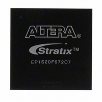
EP1S20F672C7 Altera, EP1S20F672C7 Datasheet - Page 158

EP1S20F672C7
Manufacturer Part Number
EP1S20F672C7
Description
IC STRATIX FPGA 20K LE 672-FBGA
Manufacturer
Altera
Series
Stratix®r
Datasheet
1.EP1S10F780C7.pdf
(276 pages)
Specifications of EP1S20F672C7
Number Of Logic Elements/cells
18460
Number Of Labs/clbs
1846
Total Ram Bits
1669248
Number Of I /o
426
Voltage - Supply
1.425 V ~ 1.575 V
Mounting Type
Surface Mount
Operating Temperature
0°C ~ 85°C
Package / Case
672-FBGA
Family Name
Stratix
Number Of Logic Blocks/elements
18460
# I/os (max)
426
Frequency (max)
420.17MHz
Process Technology
0.13um (CMOS)
Operating Supply Voltage (typ)
1.5V
Logic Cells
18460
Ram Bits
1669248
Operating Supply Voltage (min)
1.425V
Operating Supply Voltage (max)
1.575V
Operating Temp Range
0C to 85C
Operating Temperature Classification
Commercial
Mounting
Surface Mount
Pin Count
672
Package Type
FBGA
Lead Free Status / RoHS Status
Contains lead / RoHS non-compliant
Number Of Gates
-
Lead Free Status / Rohs Status
Not Compliant
Other names
544-1113
Available stocks
Company
Part Number
Manufacturer
Quantity
Price
Company:
Part Number:
EP1S20F672C7
Manufacturer:
SHARP
Quantity:
3 509
Company:
Part Number:
EP1S20F672C7
Manufacturer:
ALTERA
Quantity:
528
Part Number:
EP1S20F672C7
Manufacturer:
ALTERA/阿尔特拉
Quantity:
20 000
Company:
Part Number:
EP1S20F672C7N
Manufacturer:
Harting
Quantity:
1 000
Company:
Part Number:
EP1S20F672C7N
Manufacturer:
ALTERA
Quantity:
3 000
IEEE Std. 1149.1 (JTAG) Boundary-Scan Support
3–4
Stratix Device Handbook, Volume 1
Figure 3–1
Figure 3–1. Stratix JTAG Waveforms
Table 3–4
devices.
t
t
t
t
t
t
t
t
t
t
t
t
t
Captured
Symbol
JCP
JCH
JCL
JPSU
JPH
JPCO
JPZX
JPXZ
JSSU
JSH
JSCO
JSZX
JSXZ
Table 3–4. Stratix JTAG Timing Parameters & Values
Driven
Signal
Signal
to Be
to Be
TMS
TDO
TCK
TDI
shows the JTAG timing parameters and values for Stratix
TCK
TCK
TCK
JTAG port setup time
JTAG port hold time
JTAG port clock to output
JTAG port high impedance to valid output
JTAG port valid output to high impedance
Capture register setup time
Capture register hold time
Update register clock to output
Update register high impedance to valid output
Update register valid output to high impedance
shows the timing requirements for the JTAG signals.
t
clock period
clock high time
clock low time
JCH
t
t
JPZX
JSZX
t
JCP
t
JSSU
t
JCL
Parameter
t
JSH
t
t
JPCO
JSCO
t
JPSU
t
t
JSXZ
JPH
Altera Corporation
Min
100
50
50
20
45
20
45
t
JPXZ
Max
25
25
25
35
35
35
July 2005
Unit
ns
ns
ns
ns
ns
ns
ns
ns
ns
ns
ns
ns
ns


