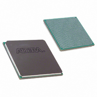
EP2S30F672I4 Altera, EP2S30F672I4 Datasheet - Page 112

EP2S30F672I4
Manufacturer Part Number
EP2S30F672I4
Description
IC STRATIX II FPGA 30K 672-FBGA
Manufacturer
Altera
Series
Stratix® IIr
Datasheet
1.EP2S15F484I4N.pdf
(238 pages)
Specifications of EP2S30F672I4
Number Of Logic Elements/cells
33880
Number Of Labs/clbs
1694
Total Ram Bits
1369728
Number Of I /o
500
Voltage - Supply
1.15 V ~ 1.25 V
Mounting Type
Surface Mount
Operating Temperature
-40°C ~ 100°C
Package / Case
672-FBGA
Family Name
Stratix II
Number Of Logic Blocks/elements
33880
# I/os (max)
500
Frequency (max)
711.24MHz
Process Technology
90nm (CMOS)
Operating Supply Voltage (typ)
1.2V
Logic Cells
33880
Ram Bits
1369728
Operating Supply Voltage (min)
1.15V
Operating Supply Voltage (max)
1.25V
Operating Temp Range
-40C to 100C
Operating Temperature Classification
Industrial
Mounting
Surface Mount
Pin Count
672
Package Type
FC-FBGA
Lead Free Status / RoHS Status
Contains lead / RoHS non-compliant
Number Of Gates
-
Lead Free Status / Rohs Status
Not Compliant
Other names
544-1899
EP2S30F672I4
EP2S30F672I4
Available stocks
Company
Part Number
Manufacturer
Quantity
Price
Company:
Part Number:
EP2S30F672I4
Manufacturer:
ALTERA
Quantity:
3 000
Company:
Part Number:
EP2S30F672I4N
Manufacturer:
ALTERA
Quantity:
238
Document Revision History
Document
Revision History
2–104
Stratix II Device Handbook, Volume 1
May 2007, v4.3 Updated
August 2006,
v4.2
April 2006,
v4.1
December
2005, v4.0
July 2005, v3.1
May 2005, v3.0
March 2005,
2.1
Table 2–27. Document Revision History (Part 1 of 2)
Document
Date and
Version
Updated note in the
Deleted Tables 2-11 and 2-12.
Updated notes to:
●
●
●
●
Updated notes to
Moved Document Revision History to end of the chapter.
Updated Table 2–18 with note.
●
●
●
●
●
Updated “Clock Control Block” section.
●
●
●
●
●
●
●
●
●
●
●
Figure 2–41
Figure 2–42
Figure 2–43
Figure 2–45
Updated Table 2–13.
Removed Note 2 from Table 2–16.
Updated “On-Chip Termination” section and Table 2–19 to
include parallel termination with calibration information.
Added new “On-Chip Parallel Termination with Calibration”
section.
Updated Figure 2–44.
Updated HyperTransport technology information in Table 2–18.
Updated HyperTransport technology information in
Figure 2–57.
Added information on the asynchronous clear signal.
Updated “Functional Description” section.
Updated Table 2–3.
Updated “Clock Control Block” section.
Updated Tables 2–17 through 2–19.
Updated Tables 2–20 through 2–22.
Updated Figure 2–57.
Updated “Functional Description” section.
Updated Table 2–3.
“Clock Control Block”
Table 2–27
Table
“Clock Control Block”
2–18.
shows the revision history for this chapter.
Changes Made
section.
section.
●
●
Summary of Changes
Added parallel on-
chip termination
description and
specification.
Changed RCLK
names to match the
Quartus II software in
Table 2–13.
Altera Corporation
—
—
—
—
—
—
—
—
—
—
—
May 2007


