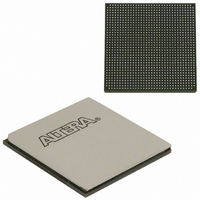
EP2SGX60EF1152I4 Altera, EP2SGX60EF1152I4 Datasheet - Page 141

EP2SGX60EF1152I4
Manufacturer Part Number
EP2SGX60EF1152I4
Description
IC STRATIX II GX 60K 1152-FBGA
Manufacturer
Altera
Series
Stratix® II GXr
Datasheet
1.EP2SGX30DF780C5.pdf
(316 pages)
Specifications of EP2SGX60EF1152I4
Number Of Logic Elements/cells
60440
Number Of Labs/clbs
3022
Total Ram Bits
2544192
Number Of I /o
534
Voltage - Supply
1.15 V ~ 1.25 V
Mounting Type
Surface Mount
Operating Temperature
-40°C ~ 100°C
Package / Case
1152-FBGA
Family Name
Stratix II GX
Number Of Logic Blocks/elements
60440
# I/os (max)
534
Frequency (max)
732.1MHz
Process Technology
SRAM
Operating Supply Voltage (typ)
1.2V
Logic Cells
60440
Ram Bits
2544192
Operating Supply Voltage (min)
1.15V
Operating Supply Voltage (max)
1.25V
Operating Temp Range
-40C to 100C
Operating Temperature Classification
Industrial
Mounting
Surface Mount
Pin Count
1152
Package Type
FC-FBGA
Lead Free Status / RoHS Status
Contains lead / RoHS non-compliant
Number Of Gates
-
Lead Free Status / Rohs Status
Not Compliant
Other names
544-2186
Available stocks
Company
Part Number
Manufacturer
Quantity
Price
Company:
Part Number:
EP2SGX60EF1152I4N
Manufacturer:
ALTERA
Quantity:
534
- Current page: 141 of 316
- Download datasheet (2Mb)
Altera Corporation
October 2007
f
f
On-Chip Parallel Termination with Calibration
Stratix II GX devices support on-chip parallel termination with
calibration for column I/O pins only. There is one calibration circuit for
the top I/O banks and one circuit for the bottom I/O banks. Each on-chip
parallel termination calibration circuit compares the total impedance of
each I/O buffer to the external 50-Ω resistors connected to the RUP and
RDN pins and dynamically enables or disables the transistors until they
match. Calibration occurs at the end of device configuration. Once the
calibration circuit finds the correct impedance, it powers down and stops
changing the characteristics of the drivers.
1
For more information about on-chip termination supported by Stratix II
devices, refer to the
Devices
For more information about tolerance specifications for on-chip
termination with calibration, refer to the
chapter in volume 1 of the Stratix II GX Device Handbook.
MultiVolt I/O Interface
The Stratix II GX architecture supports the MultiVolt I/O interface feature
that allows Stratix II GX devices in all packages to interface with systems
of different supply voltages. The Stratix II GX VCCINT pins must always
be connected to a 1.2-V power supply. With a 1.2-V V
pins are 1.2-, 1.5-, 1.8-, 2.5-, and 3.3-V tolerant. The VCCIO pins can be
connected to either a 1.2-, 1.5-, 1.8-, 2.5-, or 3.3-V power supply,
depending on the output requirements. The output levels are compatible
with systems of the same voltage as the power supply (for example, when
VCCIO pins are connected to a 1.5-V power supply, the output levels are
compatible with 1.5-V systems). The Stratix II GX VCCPD power pins
must be connected to a 3.3-V power supply. These power pins are used to
supply the pre-driver power to the output buffers, which increases the
performance of the output pins. The VCCPD pins also power
configuration input pins and JTAG input pins.
chapter in volume 2 of the Stratix II GX Device Handbook.
On-chip parallel termination with calibration is only supported
for input pins.
Selectable I/O Standards in Stratix II & Stratix II GX
Stratix II GX Device Handbook, Volume 1
DC & Switching Characteristics
Stratix II GX Architecture
CCINT
level, input
2–133
Related parts for EP2SGX60EF1152I4
Image
Part Number
Description
Manufacturer
Datasheet
Request
R

Part Number:
Description:
4. Serial Configuration Devices Epcs1, Epcs4, Epcs16, Epcs64, And Epcs128 Data Sheet
Manufacturer:
Altera Corporation
Datasheet:

Part Number:
Description:
CYCLONE II STARTER KIT EP2C20N
Manufacturer:
Altera
Datasheet:

Part Number:
Description:
CPLD, EP610 Family, ECMOS Process, 300 Gates, 16 Macro Cells, 16 Reg., 16 User I/Os, 5V Supply, 35 Speed Grade, 24DIP
Manufacturer:
Altera Corporation
Datasheet:

Part Number:
Description:
CPLD, EP610 Family, ECMOS Process, 300 Gates, 16 Macro Cells, 16 Reg., 16 User I/Os, 5V Supply, 15 Speed Grade, 24DIP
Manufacturer:
Altera Corporation
Datasheet:

Part Number:
Description:
Manufacturer:
Altera Corporation
Datasheet:

Part Number:
Description:
CPLD, EP610 Family, ECMOS Process, 300 Gates, 16 Macro Cells, 16 Reg., 16 User I/Os, 5V Supply, 30 Speed Grade, 24DIP
Manufacturer:
Altera Corporation
Datasheet:

Part Number:
Description:
High-performance, low-power erasable programmable logic devices with 8 macrocells, 10ns
Manufacturer:
Altera Corporation
Datasheet:

Part Number:
Description:
High-performance, low-power erasable programmable logic devices with 8 macrocells, 7ns
Manufacturer:
Altera Corporation
Datasheet:

Part Number:
Description:
Classic EPLD
Manufacturer:
Altera Corporation
Datasheet:

Part Number:
Description:
High-performance, low-power erasable programmable logic devices with 8 macrocells, 10ns
Manufacturer:
Altera Corporation
Datasheet:

Part Number:
Description:
Manufacturer:
Altera Corporation
Datasheet:

Part Number:
Description:
Manufacturer:
Altera Corporation
Datasheet:

Part Number:
Description:
Manufacturer:
Altera Corporation
Datasheet:


