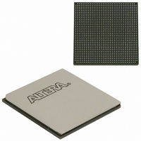
EP2SGX60EF1152I4 Altera, EP2SGX60EF1152I4 Datasheet - Page 231

EP2SGX60EF1152I4
Manufacturer Part Number
EP2SGX60EF1152I4
Description
IC STRATIX II GX 60K 1152-FBGA
Manufacturer
Altera
Series
Stratix® II GXr
Datasheet
1.EP2SGX30DF780C5.pdf
(316 pages)
Specifications of EP2SGX60EF1152I4
Number Of Logic Elements/cells
60440
Number Of Labs/clbs
3022
Total Ram Bits
2544192
Number Of I /o
534
Voltage - Supply
1.15 V ~ 1.25 V
Mounting Type
Surface Mount
Operating Temperature
-40°C ~ 100°C
Package / Case
1152-FBGA
Family Name
Stratix II GX
Number Of Logic Blocks/elements
60440
# I/os (max)
534
Frequency (max)
732.1MHz
Process Technology
SRAM
Operating Supply Voltage (typ)
1.2V
Logic Cells
60440
Ram Bits
2544192
Operating Supply Voltage (min)
1.15V
Operating Supply Voltage (max)
1.25V
Operating Temp Range
-40C to 100C
Operating Temperature Classification
Industrial
Mounting
Surface Mount
Pin Count
1152
Package Type
FC-FBGA
Lead Free Status / RoHS Status
Contains lead / RoHS non-compliant
Number Of Gates
-
Lead Free Status / Rohs Status
Not Compliant
Other names
544-2186
Available stocks
Company
Part Number
Manufacturer
Quantity
Price
Company:
Part Number:
EP2SGX60EF1152I4N
Manufacturer:
ALTERA
Quantity:
534
- Current page: 231 of 316
- Download datasheet (2Mb)
Altera Corporation
June 2009
LVTTL
LVCMOS
2.5 V
1.8 V
1.5 V
Table 4–53. Output Timing Measurement Methodology for Output Pins (Part 1 of 2)
(4)
(4)
(4)
(4)
I/O Standard
(4)
3.
4.
5.
The Quartus II software reports the timing with the conditions shown in
Table 4–53
circuit that is represented by the output timing of the Quartus II software.
Figure 4–8. Output Delay Timing Reporting Setup Modeled by Quartus II
Notes to
(1)
(2)
(3)
R
Simulate the output driver of choice into the actual PCB trace and
load, using the appropriate IBIS model or capacitance value to
represent the load.
Record the time to V
Compare the results of steps 2 and 4. The increase or decrease in
delay should be added to or subtracted from the I/O Standard
Output Adder delays to yield the actual worst-case propagation
delay (clock-to-output) of the PCB trace.
Output pin timing is reported at the output pin of the FPGA device. Additional
delays for loading and board trace delay need to be accounted for with IBIS model
simulations.
V
V
S
CCPD
CCINT
(
Ω
Output
Buffer
Figure
V
)
GND
CCIO
is 3.085 V unless otherwise specified.
is 1.12 V unless otherwise specified.
using the above equation.
R
4–8:
D
(
Output
Ω
Loading and Termination
)
V
MEAS
R
T
MEAS
(
Ω
)
R
.
S
V
CCIO
3.135
3.135
2.375
1.710
1.425
GND
V
Stratix II GX Device Handbook, Volume 1
TT
R
C
(V)
Figure 4–8
T
L
DC and Switching Characteristics
V
TT
(V)
shows the model of the
C
Notes
L
(pF)
0
0
0
0
0
Output
Output
(1), (2),
Measurement
p
n
V
1.5675
1.5675
1.1875
0.7125
MEAS
0.855
R
Point
D
(3)
(V)
4–61
Related parts for EP2SGX60EF1152I4
Image
Part Number
Description
Manufacturer
Datasheet
Request
R

Part Number:
Description:
4. Serial Configuration Devices Epcs1, Epcs4, Epcs16, Epcs64, And Epcs128 Data Sheet
Manufacturer:
Altera Corporation
Datasheet:

Part Number:
Description:
CYCLONE II STARTER KIT EP2C20N
Manufacturer:
Altera
Datasheet:

Part Number:
Description:
CPLD, EP610 Family, ECMOS Process, 300 Gates, 16 Macro Cells, 16 Reg., 16 User I/Os, 5V Supply, 35 Speed Grade, 24DIP
Manufacturer:
Altera Corporation
Datasheet:

Part Number:
Description:
CPLD, EP610 Family, ECMOS Process, 300 Gates, 16 Macro Cells, 16 Reg., 16 User I/Os, 5V Supply, 15 Speed Grade, 24DIP
Manufacturer:
Altera Corporation
Datasheet:

Part Number:
Description:
Manufacturer:
Altera Corporation
Datasheet:

Part Number:
Description:
CPLD, EP610 Family, ECMOS Process, 300 Gates, 16 Macro Cells, 16 Reg., 16 User I/Os, 5V Supply, 30 Speed Grade, 24DIP
Manufacturer:
Altera Corporation
Datasheet:

Part Number:
Description:
High-performance, low-power erasable programmable logic devices with 8 macrocells, 10ns
Manufacturer:
Altera Corporation
Datasheet:

Part Number:
Description:
High-performance, low-power erasable programmable logic devices with 8 macrocells, 7ns
Manufacturer:
Altera Corporation
Datasheet:

Part Number:
Description:
Classic EPLD
Manufacturer:
Altera Corporation
Datasheet:

Part Number:
Description:
High-performance, low-power erasable programmable logic devices with 8 macrocells, 10ns
Manufacturer:
Altera Corporation
Datasheet:

Part Number:
Description:
Manufacturer:
Altera Corporation
Datasheet:

Part Number:
Description:
Manufacturer:
Altera Corporation
Datasheet:

Part Number:
Description:
Manufacturer:
Altera Corporation
Datasheet:


