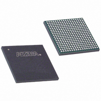
EP3C25F324I7N Altera, EP3C25F324I7N Datasheet - Page 8

EP3C25F324I7N
Manufacturer Part Number
EP3C25F324I7N
Description
IC CYCLONE III FPGA 25K 324 FBGA
Manufacturer
Altera
Series
Cyclone® IIIr
Datasheets
1.EP3C5F256C8N.pdf
(5 pages)
2.EP3C5F256C8N.pdf
(34 pages)
3.EP3C5F256C8N.pdf
(66 pages)
4.EP3C5F256C8N.pdf
(14 pages)
5.EP3C5F256C8N.pdf
(76 pages)
6.EP3C25F324I7N.pdf
(274 pages)
Specifications of EP3C25F324I7N
Number Of Logic Elements/cells
24624
Number Of Labs/clbs
1539
Total Ram Bits
608256
Number Of I /o
215
Voltage - Supply
1.15 V ~ 1.25 V
Mounting Type
Surface Mount
Operating Temperature
-40°C ~ 100°C
Package / Case
324-FBGA
Family Name
Cyclone III
Number Of Logic Blocks/elements
24624
# I/os (max)
215
Frequency (max)
437.5MHz
Process Technology
65nm
Operating Supply Voltage (typ)
1.2V
Logic Cells
24624
Ram Bits
608256
Operating Supply Voltage (min)
1.15V
Operating Supply Voltage (max)
1.25V
Operating Temp Range
-40C to 100C
Operating Temperature Classification
Industrial
Mounting
Surface Mount
Pin Count
324
Package Type
FBGA
For Use With
544-2601 - KIT DEV CYCLONE III LS EP3CLS200544-2411 - KIT DEV NIOS II CYCLONE III ED.544-2370 - KIT STARTER CYCLONE III EP3C25
Lead Free Status / RoHS Status
Lead free / RoHS Compliant
Number Of Gates
-
Lead Free Status / Rohs Status
Compliant
Other names
544-2544
Available stocks
Company
Part Number
Manufacturer
Quantity
Price
Company:
Part Number:
EP3C25F324I7N
Manufacturer:
ALTERA32
Quantity:
181
1–8
I/O Features
High-Speed Differential Interfaces
Auto-Calibrating External Memory Interfaces
Cyclone III Device Handbook, Volume 1
f
f
f
Cyclone III device family has eight I/O banks. All I/O banks support single-ended
and differential I/O standards listed in
Table 1–6. Cyclone III Device Family I/O Standards Support
The Cyclone III device family I/O also supports programmable bus hold,
programmable pull-up resistors, programmable delay, programmable drive strength,
programmable slew-rate control to optimize signal integrity, and hot socketing.
Cyclone III device family supports calibrated on-chip series termination (R
driver impedance matching (Rs) for single-ended I/O standards, with one OCT
calibration block per side.
For more information, refer to the
Cyclone III device family supports high-speed differential interfaces such as BLVDS,
LVDS, mini-LVDS, RSDS, and PPDS. These high-speed I/O standards in Cyclone III
device family provide high data throughput using a relatively small number of I/O
pins and are ideal for low-cost applications. Dedicated differential output drivers on
the left and right I/O banks can send data rates at up to 875 Mbps for Cyclone III
devices and up to 740 Mbps for Cyclone III LS devices, without the need for external
resistors. This saves board space or simplifies PCB routing. Top and bottom I/O banks
support differential transmission (with the addition of an external resistor network)
data rates at up to 640 Mbps for both Cyclone III and Cyclone III LS devices.
For more information, refer to the
chapter.
Cyclone III device family supports common memory types such as DDR, DDR2,
SDR SDRAM, and QDRII SRAM. DDR2 SDRAM memory interfaces support data
rates up to 400 Mbps for Cyclone III devices and 333 Mbps for Cyclone III LS devices.
Memory interfaces are supported on all sides of Cyclone III device family. Cyclone III
device family has the OCT, DDR output registers, and 8-to-36-bit programmable DQ
group widths features to enable rapid and robust implementation of different
memory standards.
An auto-calibrating megafunction is available in the Quartus II software for DDR and
QDR memory interface PHYs. This megafunction is optimized to take advantage of
the Cyclone III device family I/O structure, simplify timing closure requirements, and
take advantage of the Cyclone III device family PLL dynamic reconfiguration feature
to calibrate PVT changes.
For more information, refer to the
chapter.
Single-Ended I/O
Differential I/O
Type
LVTTL, LVCMOS, SSTL, HSTL, PCI, and PCI-X
SSTL, HSTL, LVPECL, BLVDS, LVDS, mini-LVDS, RSDS, and PPDS
High-Speed Differential Interfaces in Cyclone III Devices
Cyclone III Device I/O Features
External Memory Interfaces in Cyclone III Devices
Table
1–6.
I/O Standard
Chapter 1: Cyclone III Device Family Overview
© December 2009 Altera Corporation
Cyclone III Device Family Architecture
chapter.
S
OCT) or


