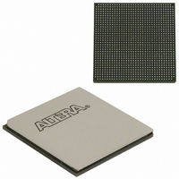
EP1AGX90EF1152I6 Altera, EP1AGX90EF1152I6 Datasheet - Page 115

EP1AGX90EF1152I6
Manufacturer Part Number
EP1AGX90EF1152I6
Description
IC ARRIA GX FPGA 90K 1152FBGA
Manufacturer
Altera
Series
Arria GXr
Datasheet
1.EP1AGX20CF484C6N.pdf
(234 pages)
Specifications of EP1AGX90EF1152I6
Number Of Logic Elements/cells
90220
Number Of Labs/clbs
4511
Total Ram Bits
4477824
Number Of I /o
538
Voltage - Supply
1.15 V ~ 1.25 V
Mounting Type
Surface Mount
Operating Temperature
-40°C ~ 100°C
Package / Case
1152-FBGA
Lead Free Status / RoHS Status
Contains lead / RoHS non-compliant
Number Of Gates
-
Available stocks
Company
Part Number
Manufacturer
Quantity
Price
Company:
Part Number:
EP1AGX90EF1152I6
Manufacturer:
ALTERA
Quantity:
8 831
Company:
Part Number:
EP1AGX90EF1152I6
Manufacturer:
ALTERA
Quantity:
3 000
Chapter 3: Configuration and Testing
SignalTap II Embedded Logic Analyzer
Table 3–3. 2-Bit Arria GX Device IDCODE
SignalTap II Embedded Logic Analyzer
Configuration
© December 2009 Altera Corporation
EP1AGX20
EP1AGX35
EP1AGX50
EP1AGX60
EP1AGX90
Device
The Arria GX device instruction register length is 10 bits and the USERCODE register
length is 32 bits.
device IDCODE information for Arria GX devices.
Table 3–2. Arria GX Boundary-Scan Register Length
Arria GX devices feature the SignalTap II embedded logic analyzer, which monitors
design operation over a period of time through the IEEE Std. 1149.1 (JTAG) circuitry.
You can analyze internal logic at speed without bringing internal signals to the I/O
pins. This feature is particularly important for advanced packages, such as FineLine
BGA (FBGA) packages, because it can be difficult to add a connection to a pin during
the debugging process after a board is designed and manufactured.
The logic, circuitry, and interconnects in the Arria GX architecture are configured with
CMOS SRAM elements. Altera
with a high coverage production test program so you do not have to perform fault
testing and can instead focus on simulation and design verification.
Arria GX devices are configured at system power up with data stored in an Altera
configuration device or provided by an external controller (for example, a MAX
device or microprocessor). You can configure Arria GX devices using the fast passive
parallel (FPP), active serial (AS), passive serial (PS), passive parallel asynchronous
(PPA), and JTAG configuration schemes. Each Arria GX device has an optimized
interface that allows microprocessors to configure it serially or in parallel, and
synchronously or asynchronously. The interface also enables microprocessors to treat
Arria GX devices as memory and configure them by writing to a virtual memory
location, making reconfiguration easy.
Version (4 Bits)
0000
0000
0000
0000
0000
EP1AGX20
EP1AGX35
EP1AGX50
EP1AGX60
EP1AGX90
Device
Table 3–2
Part Number (16 Bits)
0010 0001 0010 0001
0010 0001 0010 0001
0010 0001 0010 0010
0010 0001 0010 0010
0010 0001 0010 0011
and
®
Table 3–3
FPGAs are reconfigurable and every device is tested
IDCODE (32 Bits)
Boundary-Scan Register Length
show the boundary-scan register length and
Manufacturer Identity
000 0110 1110
000 0110 1110
000 0110 1110
000 0110 1110
000 0110 1110
1320
1320
1668
1668
2016
(11 Bits)
Arria GX Device Handbook, Volume 1
LSB (1 Bit)
1
1
1
1
1
®
II
3–3


