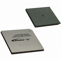
EP2S130F1508C3N Altera, EP2S130F1508C3N Datasheet - Page 177

EP2S130F1508C3N
Manufacturer Part Number
EP2S130F1508C3N
Description
IC STRATIX II FPGA 130K 1508FBGA
Manufacturer
Altera
Series
Stratix® IIr
Datasheet
1.EP2S15F484I4N.pdf
(238 pages)
Specifications of EP2S130F1508C3N
Number Of Logic Elements/cells
132540
Number Of Labs/clbs
6627
Total Ram Bits
6747840
Number Of I /o
1126
Voltage - Supply
1.15 V ~ 1.25 V
Mounting Type
Surface Mount
Operating Temperature
0°C ~ 85°C
Package / Case
1508-FBGA
Family Name
Stratix II
Number Of Logic Blocks/elements
132540
# I/os (max)
1126
Frequency (max)
778.82MHz
Process Technology
90nm (CMOS)
Operating Supply Voltage (typ)
1.2V
Logic Cells
132540
Ram Bits
6747840
Operating Supply Voltage (min)
1.15V
Operating Supply Voltage (max)
1.25V
Operating Temp Range
0C to 85C
Operating Temperature Classification
Commercial
Mounting
Surface Mount
Pin Count
1508
Package Type
FC-FBGA
Lead Free Status / RoHS Status
Lead free / RoHS Compliant
Number Of Gates
-
Lead Free Status / Rohs Status
Compliant
Other names
544-1869
EP2S130F1508C3N
Q2675539A
EP2S130F1508C3N
Q2675539A
Available stocks
Company
Part Number
Manufacturer
Quantity
Price
Company:
Part Number:
EP2S130F1508C3N
Manufacturer:
ALTERA
Quantity:
216
Part Number:
EP2S130F1508C3N
Manufacturer:
ALTERA/阿尔特拉
Quantity:
20 000
- Current page: 177 of 238
- Download datasheet (3Mb)
Altera Corporation
April 2011
Notes to
(1)
(2)
(3)
(4)
(5)
t
t
M E G A C L K H
M E G A C L R
Table 5–42. M-RAM Block Internal Timing Microparameters (Part 2 of 2)
Symbol
F
These numbers apply to -3 speed grade EP2S15, EP2S30, EP2S60, and EP2S90 devices.
These numbers apply to -3 speed grade EP2S130 and EP2S180 devices.
For the -3 and -5 speed grades, the minimum timing is for the commercial temperature grade. Only -4 speed grade
devices offer the industrial temperature grade.
For the -4 speed grade, the first number is the minimum timing parameter for industrial devices. The second
number is the minimum timing parameter for commercial devices.
MAX
Table
of M-RAM Block obtained using the Quartus II software does not necessarily equal to 1/TMEGARC.
5–42:
Minimum clock high
time
Minimum clear pulse
width
Parameter
Stratix II Clock Timing Parameters
See
t
t
t
t
C I N
C O U T
P L L C I N
P L L C O U T
Table 5–43. Stratix II Clock Timing Parameters
Tables 5–43
Symbol
1,250
Min
144
(4)
Grade
-3 Speed
through
Delay from clock pad to I/O input register
Delay from clock pad to I/O output register
Delay from PLL
Delay from PLL
Max
(2)
5–67
1,312
Min
151
(4)
Grade
-3 Speed
for Stratix II clock timing parameters.
inclk
inclk
Max
(3)
Stratix II Device Handbook, Volume 1
pad to I/O input register
pad to I/O output register
Parameter
1,437
1,437
Min
165
165
(5)
-4 Speed
DC & Switching Characteristics
Grade
Note (1)
Max
1,675
Min
192
(4)
-5 Speed
Grade
Max
5–41
Unit
ps
ps
Related parts for EP2S130F1508C3N
Image
Part Number
Description
Manufacturer
Datasheet
Request
R

Part Number:
Description:
CYCLONE II STARTER KIT EP2C20N
Manufacturer:
Altera
Datasheet:

Part Number:
Description:
CPLD, EP610 Family, ECMOS Process, 300 Gates, 16 Macro Cells, 16 Reg., 16 User I/Os, 5V Supply, 35 Speed Grade, 24DIP
Manufacturer:
Altera Corporation
Datasheet:

Part Number:
Description:
CPLD, EP610 Family, ECMOS Process, 300 Gates, 16 Macro Cells, 16 Reg., 16 User I/Os, 5V Supply, 15 Speed Grade, 24DIP
Manufacturer:
Altera Corporation
Datasheet:

Part Number:
Description:
Manufacturer:
Altera Corporation
Datasheet:

Part Number:
Description:
CPLD, EP610 Family, ECMOS Process, 300 Gates, 16 Macro Cells, 16 Reg., 16 User I/Os, 5V Supply, 30 Speed Grade, 24DIP
Manufacturer:
Altera Corporation
Datasheet:

Part Number:
Description:
High-performance, low-power erasable programmable logic devices with 8 macrocells, 10ns
Manufacturer:
Altera Corporation
Datasheet:

Part Number:
Description:
High-performance, low-power erasable programmable logic devices with 8 macrocells, 7ns
Manufacturer:
Altera Corporation
Datasheet:

Part Number:
Description:
Classic EPLD
Manufacturer:
Altera Corporation
Datasheet:

Part Number:
Description:
High-performance, low-power erasable programmable logic devices with 8 macrocells, 10ns
Manufacturer:
Altera Corporation
Datasheet:

Part Number:
Description:
Manufacturer:
Altera Corporation
Datasheet:

Part Number:
Description:
Manufacturer:
Altera Corporation
Datasheet:

Part Number:
Description:
Manufacturer:
Altera Corporation
Datasheet:

Part Number:
Description:
CPLD, EP610 Family, ECMOS Process, 300 Gates, 16 Macro Cells, 16 Reg., 16 User I/Os, 5V Supply, 25 Speed Grade, 24DIP
Manufacturer:
Altera Corporation
Datasheet:


