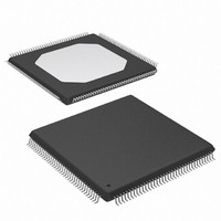
XA3S100E-4TQG144Q Xilinx Inc, XA3S100E-4TQG144Q Datasheet - Page 21

XA3S100E-4TQG144Q
Manufacturer Part Number
XA3S100E-4TQG144Q
Description
IC FPGA SPARTAN-3E 100K 144-TQFP
Manufacturer
Xilinx Inc
Series
Spartan™-3E XAr
Datasheet
1.XA3S100E-4VQG100I.pdf
(37 pages)
Specifications of XA3S100E-4TQG144Q
Number Of Logic Elements/cells
2160
Number Of Labs/clbs
240
Total Ram Bits
73728
Number Of I /o
108
Number Of Gates
100000
Voltage - Supply
1.14 V ~ 1.26 V
Mounting Type
Surface Mount
Operating Temperature
-40°C ~ 125°C
Package / Case
144-LQFP
Lead Free Status / RoHS Status
Lead free / RoHS Compliant
Available stocks
Company
Part Number
Manufacturer
Quantity
Price
Company:
Part Number:
XA3S100E-4TQG144Q
Manufacturer:
XILINX
Quantity:
2 960
Company:
Part Number:
XA3S100E-4TQG144Q
Manufacturer:
Xilinx Inc
Quantity:
10 000
Table 21: CLB Distributed RAM Switching Characteristics
Table 22: CLB Shift Register Switching Characteristics
DS635 (v2.0) September 9, 2009
Product Specification
Clock-to-Output Times
Setup Times
Hold Times
Clock Pulse Width
Clock-to-Output Times
Setup Times
Hold Times
Clock Pulse Width
T
T
WPH
WPH
T
Symbol
Symbol
T
T
T
AH,
T
SRLDH
SHCKO
SRLDS
T
T
T
T
REG
WS
, T
DS
AS
DH
, T
T
WH
WPL
WPL
R
Time from the active edge at the CLK input to data appearing on the shift
register output
Setup time of data at the BX or BY input before the active transition at the
CLK input of the shift register
Hold time of the BX or BY data input after the active transition at the CLK
input of the shift register
Minimum High or Low pulse width at CLK input
Time from the active edge at the CLK input to data appearing on the
distributed RAM output
Setup time of data at the BX or BY input before the active transition at the
CLK input of the distributed RAM
Setup time of the F/G address inputs before the active transition at the CLK
input of the distributed RAM
Setup time of the write enable input before the active transition at the CLK
input of the distributed RAM
Hold time of the BX, BY data inputs after the active transition at the CLK
input of the distributed RAM
Hold time of the F/G address inputs or the write enable input after the active
transition at the CLK input of the distributed RAM
Minimum High or Low pulse width at CLK input
Description
Description
www.xilinx.com
0.46
0.52
0.40
0.15
1.01
Min
0.46
0.16
1.01
Min
0
-
-
-4
-4
Max
2.35
Max
4.16
-
-
-
-
-
-
-
-
-
Units
Units
ns
ns
ns
ns
ns
ns
ns
ns
ns
ns
ns
21


