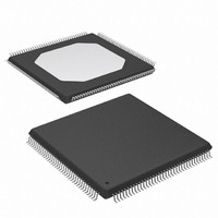
XA3S100E-4TQG144Q Xilinx Inc, XA3S100E-4TQG144Q Datasheet - Page 33

XA3S100E-4TQG144Q
Manufacturer Part Number
XA3S100E-4TQG144Q
Description
IC FPGA SPARTAN-3E 100K 144-TQFP
Manufacturer
Xilinx Inc
Series
Spartan™-3E XAr
Datasheet
1.XA3S100E-4VQG100I.pdf
(37 pages)
Specifications of XA3S100E-4TQG144Q
Number Of Logic Elements/cells
2160
Number Of Labs/clbs
240
Total Ram Bits
73728
Number Of I /o
108
Number Of Gates
100000
Voltage - Supply
1.14 V ~ 1.26 V
Mounting Type
Surface Mount
Operating Temperature
-40°C ~ 125°C
Package / Case
144-LQFP
Lead Free Status / RoHS Status
Lead free / RoHS Compliant
Available stocks
Company
Part Number
Manufacturer
Quantity
Price
Company:
Part Number:
XA3S100E-4TQG144Q
Manufacturer:
XILINX
Quantity:
2 960
Company:
Part Number:
XA3S100E-4TQG144Q
Manufacturer:
Xilinx Inc
Quantity:
10 000
Serial Peripheral Interface Configuration Timing
Table 40: Timing for SPI Configuration Mode
Table 41: Configuration Timing Requirements for Attached SPI Serial Flash
DS635 (v2.0) September 9, 2009
Product Specification
Notes:
1.
2.
T
T
T
T
T
T
T
T
T
T
T
f
C
Symbol
CCLK1
CCLKn
MINIT
INITM
CCO
DCC
CCD
CCS
DSU
DH
V
Symbol
or f
These requirements are for successful FPGA configuration in SPI mode, where the FPGA provides the CCLK frequency. The post
configuration timing can be different to support the specific needs of the application loaded into the FPGA and the resulting clock source.
Subtract additional printed circuit board routing delay as required by the application.
R
R
SPI serial Flash PROM chip-select time
SPI serial Flash PROM data input setup time
SPI serial Flash PROM data input hold time
SPI serial Flash PROM data clock-to-output time
Maximum SPI serial Flash PROM clock frequency (also depends
on specific read command used)
Initial CCLK clock period
CCLK clock period after FPGA loads ConfigRate setting
Setup time on VS[2:0] and M[2:0] mode pins before the rising
edge of INIT_B
Hold time on VS[2:0] and M[2:0]mode pins after the rising edge of
INIT_B
MOSI output valid after CCLK edge
Setup time on DIN data input before CCLK edge
Hold time on DIN data input after CCLK edge
Description
Description
www.xilinx.com
T
T
T
Minimum
CCS
V
DSU
f
C
T
≤
50
0
≥
DH
T
Requirement
≤
≤
MCCLn
------------------------------ -
T
T
≤
T
CCLKn min
MCCL1
MCCL1
(see
(see
T
See
See
See
MCCH1
1
Maximum
–
Table
Table
Table 38
Table 38
Table 38
(
T
–
–
DCC
-
-
T
T
)
CCO
34)
34)
CCO
Units
Units
MHz
ns
ns
ns
ns
ns
ns
33


