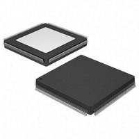
XC3S500E-4PQG208I Xilinx Inc, XC3S500E-4PQG208I Datasheet - Page 46

XC3S500E-4PQG208I
Manufacturer Part Number
XC3S500E-4PQG208I
Description
IC FPGA SPARTAN-3E 500K 208-PQFP
Manufacturer
Xilinx Inc
Series
Spartan™-3Er
Datasheet
1.XC3S100E-4VQG100C.pdf
(233 pages)
Specifications of XC3S500E-4PQG208I
Package / Case
208-MQFP, 208-PQFP
Mounting Type
Surface Mount
Voltage - Supply
1.1 V ~ 3.465 V
Operating Temperature
-40°C ~ 100°C
Number Of I /o
158
Number Of Logic Elements/cells
*
Number Of Gates
*
No. Of Logic Blocks
1564
No. Of Gates
500000
No. Of Macrocells
10476
Family Type
Spartan-3E
No. Of Speed Grades
4
No. Of I/o's
158
Clock
RoHS Compliant
Total Ram Bits
368640
Lead Free Status / RoHS Status
Lead free / RoHS Compliant
Available stocks
Company
Part Number
Manufacturer
Quantity
Price
Company:
Part Number:
XC3S500E-4PQG208I
Manufacturer:
Xilinx Inc
Quantity:
10 000
- Current page: 46 of 233
- Download datasheet (6Mb)
Functional Description
The BCIN and BCOUT ports have associated dedicated
routing that connects adjacent multipliers within the same
column. Via the cascade connection, the BCOUT port of
one multiplier block drives the BCIN port of the multiplier
block directly above it. There is no connection to the BCIN
port of the bottom-most multiplier block in a column or a
connection from the BCOUT port of the top-most block in a
column. As an example,
cade capability within the XC3S100E FPGA, which has a
single column of multiplier, four blocks tall. For clarity, the
figure omits the register control inputs.
46
Figure 39: Multiplier Cascade Connection
B_INPUT = CASCADE
B_INPUT = CASCADE
B_INPUT = CASCADE
B_INPUT = DIRECT
Figure 39
A
B
A
B
A
B
A
B
BCOUT
BCOUT
BCOUT
BCOUT
shows the multiplier cas-
BCIN
BCIN
BCIN
BCIN
DS312-2_30_021505
P
P
P
P
www.xilinx.com
When using the BREG register, the cascade connection
forms a shift register structure typically used in DSP algo-
rithms such as direct-form FIR filters. When the BREG reg-
ister is omitted, the cascade structure essentially feeds the
same input value to more than one multiplier. This parallel
connection serves to create wide-input multipliers, imple-
ment transpose FIR filters, and is used in any application
that requires that several multipliers have the same input
value.
Multiplier/Block RAM Interaction
Each multiplier is located adjacent to an 18 Kbit block RAM
and shares some interconnect resources. Configuring an
18 Kbit block RAM for 36-bit wide data (512 x 36 mode) pre-
vents use of the associated dedicated multiplier.
The upper 16 bits of the ‘A’ multiplicand input are shared
with the upper 16 bits of the block RAM’s Port A Data input.
Similarly, the upper 16 bits of the ‘B’ multiplicand input are
shared with Port B’s data input. See also
page
64.
DS312-2 (v3.8) August 26, 2009
Product Specification
Figure 48,
R
Related parts for XC3S500E-4PQG208I
Image
Part Number
Description
Manufacturer
Datasheet
Request
R

Part Number:
Description:
IC SPARTAN-3E FPGA 500K 320FBGA
Manufacturer:
Xilinx Inc
Datasheet:

Part Number:
Description:
IC FPGA SPARTAN-3E 500K 132CSBGA
Manufacturer:
Xilinx Inc
Datasheet:

Part Number:
Description:
IC FPGA SPARTAN-3E 500K 256FTBGA
Manufacturer:
Xilinx Inc
Datasheet:

Part Number:
Description:
IC FPGA SPARTAN-3E 500K 256FTBGA
Manufacturer:
Xilinx Inc
Datasheet:

Part Number:
Description:
IC FPGA SPARTAN-3E 500K 320-FBGA
Manufacturer:
Xilinx Inc
Datasheet:

Part Number:
Description:
IC FPGA SPARTAN 3E 320FBGA
Manufacturer:
Xilinx Inc
Datasheet:

Part Number:
Description:
FPGA Spartan®-3E Family 500K Gates 10476 Cells 572MHz 90nm (CMOS) Technology 1.2V 256-Pin FTBGA
Manufacturer:
Xilinx Inc
Datasheet:

Part Number:
Description:
FPGA Spartan®-3E Family 500K Gates 10476 Cells 572MHz 90nm (CMOS) Technology 1.2V 208-Pin PQFP
Manufacturer:
Xilinx Inc
Datasheet:

Part Number:
Description:
FPGA Spartan®-3E Family 500K Gates 10476 Cells 572MHz 90nm (CMOS) Technology 1.2V 208-Pin PQFP
Manufacturer:
Xilinx Inc
Datasheet:

Part Number:
Description:
FPGA Spartan®-3E Family 500K Gates 10476 Cells 572MHz 90nm (CMOS) Technology 1.2V 256-Pin FTBGA
Manufacturer:
Xilinx Inc
Datasheet:

Part Number:
Description:
FPGA Spartan®-3E Family 500K Gates 10476 Cells 572MHz 90nm (CMOS) Technology 1.2V 132-Pin CSBGA
Manufacturer:
Xilinx Inc
Datasheet:

Part Number:
Description:
FPGA Spartan-3E Family 500K Gates 10476 Cells 572MHz 90nm (CMOS) Technology 1.2V 320-Pin FBGA
Manufacturer:
Xilinx Inc
Datasheet:

Part Number:
Description:
IC FPGA SPARTAN-3E 500K 100-VQFP
Manufacturer:
Xilinx Inc
Datasheet:

Part Number:
Description:
IC FPGA SPARTAN-3E 500K 132CSBGA
Manufacturer:
Xilinx Inc
Datasheet:

Part Number:
Description:
IC FPGA SPARTAN-3E 500K 320-FBGA
Manufacturer:
Xilinx Inc
Datasheet:


