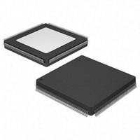
XC3S500E-4PQG208I Xilinx Inc, XC3S500E-4PQG208I Datasheet - Page 63

XC3S500E-4PQG208I
Manufacturer Part Number
XC3S500E-4PQG208I
Description
IC FPGA SPARTAN-3E 500K 208-PQFP
Manufacturer
Xilinx Inc
Series
Spartan™-3Er
Datasheet
1.XC3S100E-4VQG100C.pdf
(233 pages)
Specifications of XC3S500E-4PQG208I
Package / Case
208-MQFP, 208-PQFP
Mounting Type
Surface Mount
Voltage - Supply
1.1 V ~ 3.465 V
Operating Temperature
-40°C ~ 100°C
Number Of I /o
158
Number Of Logic Elements/cells
*
Number Of Gates
*
No. Of Logic Blocks
1564
No. Of Gates
500000
No. Of Macrocells
10476
Family Type
Spartan-3E
No. Of Speed Grades
4
No. Of I/o's
158
Clock
RoHS Compliant
Total Ram Bits
368640
Lead Free Status / RoHS Status
Lead free / RoHS Compliant
Available stocks
Company
Part Number
Manufacturer
Quantity
Price
Company:
Part Number:
XC3S500E-4PQG208I
Manufacturer:
Xilinx Inc
Quantity:
10 000
- Current page: 63 of 233
- Download datasheet (6Mb)
The outputs of the top or bottom BUFGMUX elements con-
nect to two vertical spines, each comprising four vertical
clock lines as shown in
these clock signals connect to the eight-line horizontal clock
spine.
Outputs of the left and right BUFGMUX elements are routed
onto the left or right horizontal spines, each comprising
eight horizontal clock lines.
Each of the eight clock signals in a clock quadrant derives
either from a global clock signal or a half clock signal. In
other words, there are up to 24 total potential clock inputs to
the FPGA, eight of which can connect to clocked elements
DS312-2 (v3.8) August 26, 2009
Product Specification
R
Figure 47: Clock Sources for the Eight Clock Lines within a Clock Quadrant
a. Left (TL and BL Quadrants) Half of Die
BUFGMUX Output
X0Y9 (Left Half)
X0Y8 (Left Half)
X0Y7 (Left Half)
X0Y6 (Left Half)
X0Y5 (Left Half)
X0Y4 (Left Half)
X0Y3 (Left Half)
X0Y2 (Left Half)
X1Y10 (Global)
X1Y11 (Global)
X2Y10 (Global)
X2Y11 (Global)
X1Y0 (Global)
X1Y1 (Global)
X2Y0 (Global)
X2Y1 (Global)
Figure
45. At the center of the die,
Clock Line
H
G
F
E
D
C
B
A
www.xilinx.com
b. Right (TR and BR Quadrants) Half of Die
X3Y9 (Right Half)
X3Y8 (Right Half)
X3Y7 (Right Half)
X3Y6 (Right Half)
X3Y5 (Right Half)
X3Y4 (Right Half)
X3Y3 (Right Half)
X3Y2 (Right Half)
BUFGMUX Output
in a single clock quadrant.
lines in each quadrant are selected from associated BUFG-
MUX sources. For example, if quadrant clock ‘A’ in the bot-
tom left (BL) quadrant originates from BUFGMUX_X2Y1,
then the clock signal from BUFGMUX_X0Y2 is unavailable
in the bottom left quadrant. However, the top left (TL) quad-
rant clock ‘A’ can still solely use the output from either
BUFGMUX_X2Y1 or BUFGMUX_X0Y2 as the source.
To minimize the dynamic power dissipation of the clock net-
work, the Xilinx development software automatically dis-
ables all clock segments not in use.
X1Y10 (Global)
X1Y11 (Global)
X2Y10 (Global)
X2Y11 (Global)
X1Y0 (Global)
X1Y1 (Global)
X2Y0 (Global)
X2Y1 (Global)
DS312-2_17_103105
Figure 47
Clock Line
H
G
F
E
D
C
B
A
Functional Description
shows how the clock
63
Related parts for XC3S500E-4PQG208I
Image
Part Number
Description
Manufacturer
Datasheet
Request
R

Part Number:
Description:
IC SPARTAN-3E FPGA 500K 320FBGA
Manufacturer:
Xilinx Inc
Datasheet:

Part Number:
Description:
IC FPGA SPARTAN-3E 500K 132CSBGA
Manufacturer:
Xilinx Inc
Datasheet:

Part Number:
Description:
IC FPGA SPARTAN-3E 500K 256FTBGA
Manufacturer:
Xilinx Inc
Datasheet:

Part Number:
Description:
IC FPGA SPARTAN-3E 500K 256FTBGA
Manufacturer:
Xilinx Inc
Datasheet:

Part Number:
Description:
IC FPGA SPARTAN-3E 500K 320-FBGA
Manufacturer:
Xilinx Inc
Datasheet:

Part Number:
Description:
IC FPGA SPARTAN 3E 320FBGA
Manufacturer:
Xilinx Inc
Datasheet:

Part Number:
Description:
FPGA Spartan®-3E Family 500K Gates 10476 Cells 572MHz 90nm (CMOS) Technology 1.2V 256-Pin FTBGA
Manufacturer:
Xilinx Inc
Datasheet:

Part Number:
Description:
FPGA Spartan®-3E Family 500K Gates 10476 Cells 572MHz 90nm (CMOS) Technology 1.2V 208-Pin PQFP
Manufacturer:
Xilinx Inc
Datasheet:

Part Number:
Description:
FPGA Spartan®-3E Family 500K Gates 10476 Cells 572MHz 90nm (CMOS) Technology 1.2V 208-Pin PQFP
Manufacturer:
Xilinx Inc
Datasheet:

Part Number:
Description:
FPGA Spartan®-3E Family 500K Gates 10476 Cells 572MHz 90nm (CMOS) Technology 1.2V 256-Pin FTBGA
Manufacturer:
Xilinx Inc
Datasheet:

Part Number:
Description:
FPGA Spartan®-3E Family 500K Gates 10476 Cells 572MHz 90nm (CMOS) Technology 1.2V 132-Pin CSBGA
Manufacturer:
Xilinx Inc
Datasheet:

Part Number:
Description:
FPGA Spartan-3E Family 500K Gates 10476 Cells 572MHz 90nm (CMOS) Technology 1.2V 320-Pin FBGA
Manufacturer:
Xilinx Inc
Datasheet:

Part Number:
Description:
IC FPGA SPARTAN-3E 500K 100-VQFP
Manufacturer:
Xilinx Inc
Datasheet:

Part Number:
Description:
IC FPGA SPARTAN-3E 500K 132CSBGA
Manufacturer:
Xilinx Inc
Datasheet:

Part Number:
Description:
IC FPGA SPARTAN-3E 500K 320-FBGA
Manufacturer:
Xilinx Inc
Datasheet:


