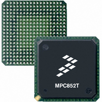
MPC852TCVR66A Freescale Semiconductor, MPC852TCVR66A Datasheet - Page 13

MPC852TCVR66A
Manufacturer Part Number
MPC852TCVR66A
Description
IC MPU POWERQUICC 66MHZ 256PBGA
Manufacturer
Freescale Semiconductor
Datasheet
1.MPC852TVR50A.pdf
(80 pages)
Specifications of MPC852TCVR66A
Processor Type
MPC8xx PowerQUICC 32-Bit
Speed
66MHz
Voltage
1.8V
Mounting Type
Surface Mount
Package / Case
256-PBGA
Processor Series
MPC8xx
Core
MPC8xx
Data Bus Width
32 bit
Development Tools By Supplier
MPC852TADS-KIT
Maximum Clock Frequency
66 MHz
Operating Supply Voltage
1.8 V, 3.3 V
Maximum Operating Temperature
+ 105 C
Mounting Style
SMD/SMT
Minimum Operating Temperature
- 40 C
Family Name
MPC8xx
Device Core
PowerQUICC
Device Core Size
32b
Frequency (max)
66MHz
Instruction Set Architecture
RISC
Supply Voltage 1 (typ)
1.8/3.3V
Operating Supply Voltage (max)
1.9/3.465V
Operating Supply Voltage (min)
1.7/3.135V
Operating Temp Range
-40C to 100C
Operating Temperature Classification
Industrial
Mounting
Surface Mount
Pin Count
256
Package Type
BGA
Lead Free Status / RoHS Status
Lead free / RoHS Compliant
Features
-
Lead Free Status / Rohs Status
Lead free / RoHS Compliant
Available stocks
Company
Part Number
Manufacturer
Quantity
Price
Company:
Part Number:
MPC852TCVR66A
Manufacturer:
Freescale Semiconductor
Quantity:
10 000
The MBMR[GPLB4DIS], PAPAR, PADIR, PBPAR, PBDIR, PCPAR, and PCDIR should be configured
with the mandatory value in
11 Layout Practices
Each V
GND pin should likewise be provided with a low-impedance path to ground. The power supply pins drive
distinct groups of logic on chip. The V
0.1 µF bypass capacitors located as close as possible to the four sides of the package. Each board designed
should be characterized and additional appropriate decoupling capacitors should be used if required. The
capacitor leads and associated printed-circuit traces connecting to chip V
less than half an inch per capacitor lead. At a minimum, a four-layer board employing two inner layers as
V
All output pins on the MPC852T have fast rise and fall times. Printed-circuit (PC) trace interconnection
length should be minimized to minimize undershoot and reflections that these fast output switching times
cause. This recommendation particularly applies to the address and data buses. Maximum PC trace lengths
of six inches are recommended. Capacitance calculations should consider all device loads as well as
parasitic capacitances that the PC traces cause. Attention to proper PCB layout and bypassing becomes
especially critical in systems with higher capacitive loads, because these loads create higher transient
currents in the V
Special care should be taken to minimize the noise levels on the PLL supply pins. For more information,
please refer to the MPC866 PowerQUICC™ Family Reference Manual, Section 14.4.3, “Clock
Synthesizer Power (V
Freescale Semiconductor
DD
and GND planes should be used.
DD
pin on the MPC852T should be provided with a low-impedance path to the board’s supply. Each
HRCW (Hardware reset configuration word)
SIUMCR (SIU module configuration register)
MBMR (Machine B mode register)
PAPAR (Port A pin assignment register)
PADIR (Port A data direction register)
PBPAR (Port B pin assignment register)
PBDIR (Port B data direction register)
PCPAR (Port C pin assignment register)
PCDIR (Port C data direction register)
DD
and GND circuits. Pull up all unused inputs or signals that are inputs during reset.
DDSYN
Register/Configuration
Table 6. Mandatory Reset Configuration of MPC852T
MPC852T PowerQUICC™ Hardware Specifications, Rev. 4
Table 6
, V
SSSYN
in the boot code after the reset deasserts.
, V
DD
SSSYN1
power supply should be bypassed to ground using at least four
).”
HRCW[DBGC]
SIUMCR[DBGC]
PAPAR[4–7]
MBMR[GPLB4DIS}
PAPAR[12–15]
PADIR[4–7]
PADIR[12–15]
PBPAR[14]
PBPAR[16–23]
PBPAR[26–27]
PBDIR[14]
PBDIR[16–23]
PBDIR[26–27]
PCPAR[8–11]
PCDIR[14]
PCDIR[8–11]
PCDIR[14]
Field
DD
and GND should be kept to
(Binary)
Value
X1
X1
0
0
1
0
1
0
1
Layout Practices
13


