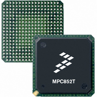
MPC852TCVR66A Freescale Semiconductor, MPC852TCVR66A Datasheet - Page 17

MPC852TCVR66A
Manufacturer Part Number
MPC852TCVR66A
Description
IC MPU POWERQUICC 66MHZ 256PBGA
Manufacturer
Freescale Semiconductor
Datasheet
1.MPC852TVR50A.pdf
(80 pages)
Specifications of MPC852TCVR66A
Processor Type
MPC8xx PowerQUICC 32-Bit
Speed
66MHz
Voltage
1.8V
Mounting Type
Surface Mount
Package / Case
256-PBGA
Processor Series
MPC8xx
Core
MPC8xx
Data Bus Width
32 bit
Development Tools By Supplier
MPC852TADS-KIT
Maximum Clock Frequency
66 MHz
Operating Supply Voltage
1.8 V, 3.3 V
Maximum Operating Temperature
+ 105 C
Mounting Style
SMD/SMT
Minimum Operating Temperature
- 40 C
Family Name
MPC8xx
Device Core
PowerQUICC
Device Core Size
32b
Frequency (max)
66MHz
Instruction Set Architecture
RISC
Supply Voltage 1 (typ)
1.8/3.3V
Operating Supply Voltage (max)
1.9/3.465V
Operating Supply Voltage (min)
1.7/3.135V
Operating Temp Range
-40C to 100C
Operating Temperature Classification
Industrial
Mounting
Surface Mount
Pin Count
256
Package Type
BGA
Lead Free Status / RoHS Status
Lead free / RoHS Compliant
Features
-
Lead Free Status / Rohs Status
Lead free / RoHS Compliant
Available stocks
Company
Part Number
Manufacturer
Quantity
Price
Company:
Part Number:
MPC852TCVR66A
Manufacturer:
Freescale Semiconductor
Quantity:
10 000
Freescale Semiconductor
B24a
B27a
B28a
B28b
B28d
B29a
Num
B28c
B25
B26
B27
B28
B29
A(0:31) and BADDR(28:30) to CS
asserted GPCM ACS = 11 TRLX = 0
(MIN = 0.50 × B1 – 2.00)
CLKOUT rising edge to OE,
WE(0:3)/BS_B[0:3] asserted
(MAX = 0.00 × B1 + 9.00)
CLKOUT rising edge to OE negated
(MAX = 0.00 × B1 + 9.00)
A(0:31) and BADDR(28:30) to CS
asserted GPCM ACS = 10, TRLX = 1
(MIN = 1.25 × B1 – 2.00)
A(0:31) and BADDR(28:30) to CS
asserted GPCM ACS = 11, TRLX = 1
(MIN = 1.50 × B1 – 2.00)
CLKOUT rising edge to WE(0:3)/
BS_B[0:3] negated GPCM write access
CSNT = 0 (MAX = 0.00 × B1 + 9.00)
CLKOUT falling edge to WE(0:3)/
BS_B[0:3] negated GPCM write access
TRLX = 0,1 CSNT = 1, EBDF = 0
(MAX = 0.25 × B1 + 6.80)
CLKOUT falling edge to CS negated
GPCM write access TRLX = 0,1 CSNT = 1
ACS = 10 or ACS = 11, EBDF = 0
(MAX = 0.25 × B1 + 6.80)
CLKOUT falling edge to
WE(0:3)/BS_B[0:3] negated GPCM write
access TRLX = 0,1 CSNT = 1 write access
TRLX = 0,1 CSNT = 1, EBDF = 1
(MAX = 0.375 × B1 + 6.6)
CLKOUT falling edge to CS negated
GPCM write access TRLX = 0,1 CSNT =
1, ACS = 10, or ACS = 11, EBDF = 1
(MAX = 0.375 × B1 + 6.6)
WE(0:3)/BS_B[0:3] negated to D(0:31),
DP(0:3) High-Z GPCM write access,
CSNT = 0, EBDF = 0
(MIN = 0.25 × B1 – 2.00)
WE(0:3)/BS_B[0:3] negated to D(0:31),
DP(0:3) High-Z GPCM write access, TRLX
= 0, CSNT = 1, EBDF = 0
(MIN = 0.50 × B1 – 2.00)
Characteristic
MPC852T PowerQUICC™ Hardware Specifications, Rev. 4
Table 9. Bus Operation Timings (continued)
13.20
35.90
43.50
10.90
13.20
2.00
7.60
5.60
Min
—
—
—
—
33 MHz
14.30
14.30
18.00
18.00
Max
9.00
9.00
9.00
—
—
—
—
—
10.50
29.30
35.50
10.90
10.50
2.00
6.30
4.30
Min
—
—
—
40 MHz
13.00
13.00
18.00
18.00
Max
9.00
9.00
9.00
—
—
—
—
—
23.00
28.00
8.00
2.00
5.00
7.00
3.00
8.00
Min
—
—
—
50 MHz
11.80
11.80
14.30
14.30
Max
9.00
9.00
9.00
—
—
—
—
—
16.90
20.70
5.60
3.80
5.20
1.80
5.60
2.00
Min
—
—
—
66 MHz
Bus Signal Timing
10.50
10.50
12.30
12.30
Max
9.00
9.00
9.00
—
—
—
—
—
Unit
ns
ns
ns
ns
ns
ns
ns
ns
ns
ns
ns
ns
17


