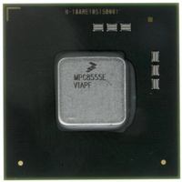
MPC8555EVTAPF Freescale Semiconductor, MPC8555EVTAPF Datasheet - Page 44

MPC8555EVTAPF
Manufacturer Part Number
MPC8555EVTAPF
Description
IC MPU POWERQUICC III 783-FCPBGA
Manufacturer
Freescale Semiconductor
Datasheet
1.MPC8555ECVTALF.pdf
(88 pages)
Specifications of MPC8555EVTAPF
Processor Type
MPC85xx PowerQUICC III 32-Bit
Speed
833MHz
Voltage
1.2V
Mounting Type
Surface Mount
Package / Case
783-FCPBGA
For Use With
MPC8555CDS - BOARD EVALUATION CDS FOR 8555CWH-PPC-8555N-VX - BOARD EVAL QUICCSTART MPC8555CWH-PPC-8540N-VE - KIT EVAL SYSTEM MPC8540CWH-PPC-8555N-VE - EVALUATION SYSTEM QUICC MPC8555E
Lead Free Status / RoHS Status
Not applicable / RoHS Compliant
Features
-
Available stocks
Company
Part Number
Manufacturer
Quantity
Price
Company:
Part Number:
MPC8555EVTAPF
Manufacturer:
Freescale Semiconductor
Quantity:
10 000
Part Number:
MPC8555EVTAPF
Manufacturer:
FREESCALE
Quantity:
20 000
CPM
Figure 23
44
FCC outputs—internal clock (NMSI) delay
FCC outputs—external clock (NMSI) delay
SCC/SMC/SPI outputs—internal clock (NMSI) delay
SCC/SMC/SPI outputs—external clock (NMSI) delay
TDM outputs/SI delay
PIO outputs delay
Notes:
1. Output specifications are measured from the 50% level of the rising edge of CLKIN to the 50% level of the signal. Timings
2. The symbols used for timing specifications follow the pattern of t
TDM inputs/SI—hold time
PIO inputs—input setup time
PIO inputs—input hold time
COL width high (FCC)
Notes:
1. Input specifications are measured from the 50% level of the signal to the 50% level of the rising edge of CLKIN. Timings
2. The symbols used for timing specifications herein follow the pattern of t
3. PIO and TIMER inputs and outputs are asynchronous to SYSCLK or any other externally visible clock. PIO/TIMER inputs
are measured at the pin.
inputs and t
inputs internal timing (FI) for the time t
invalid (X).
are measured at the pin.
(reference)(state)
symbolizes the FCC inputs internal timing (FI) with respect to the time the input signals (I) reaching the valid state (V)
relative to the reference clock t
(TD) with respect to the time the input signals (I) reach the invalid state (X) relative to the reference clock t
the high (H) state or hold time.
are internally synchronized to the CPM internal clock. PIO/TIMER outputs should be treated as asynchronous.
MPC8555E PowerQUICC™ III Integrated Communications Processor Hardware Specification, Rev. 4.2
provides the AC test load for the CPM.
(first two letters of functional block)(reference)(state)(signal)(state)
for inputs and t
Output
Table 33. CPM Input AC Timing Specifications
Characteristic
(first two letters of functional block)(reference)(state)(signal)(state)
Table 34. CPM Output AC Timing Specifications
FCC
Characteristic
(K) going to the high (H) state or setup time. And t
FCC
memory clock reference (K) goes from the high state (H) until outputs (O) are
Figure 23. CPM AC Test Load
Z
0
= 50 Ω
(first two letters of functional block)(signal)(state) (reference)(state)
for outputs. For example, t
(first two letters of functional block)(signal)(state)
R
Symbol
L
t
t
t
t
t
t
FEKHOX
NEKHOX
TDKHOX
NIKHOX
FIKHOX
PIKHOX
= 50 Ω
1
(continued)
2
for outputs. For example, t
TDIXKH
Symbol
t
OV
t
t
TDIXKH
1
t
PIIVKH
PIIXKH
FCCH
DD
FIKHOX
Min
0.5
2.5
symbolizes the TDM timing
1
2
2
1
/2
2
Freescale Semiconductor
symbolizes the FCC
Min
Max
1.5
5.5
10
11
11
3
8
1
8
8
FCC
3
FIIVKH
(K) going to
Unit
CLK
Unit
ns
ns
ns
ns
ns
ns
ns
ns
ns
for


