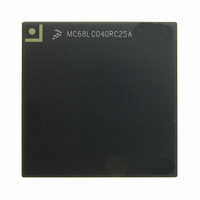
MC68LC040RC25A Freescale Semiconductor, MC68LC040RC25A Datasheet - Page 174

MC68LC040RC25A
Manufacturer Part Number
MC68LC040RC25A
Description
IC MPU 32BIT 25MHZ 179-PGA
Manufacturer
Freescale Semiconductor
Datasheet
1.MC68EC040FE33A.pdf
(442 pages)
Specifications of MC68LC040RC25A
Processor Type
M680x0 32-Bit
Speed
25MHz
Voltage
5V
Mounting Type
Surface Mount
Package / Case
179-PGA
Lead Free Status / RoHS Status
Lead free / RoHS Compliant
Features
-
Available stocks
Company
Part Number
Manufacturer
Quantity
Price
Company:
Part Number:
MC68LC040RC25A
Manufacturer:
MOT
Quantity:
6 100
Company:
Part Number:
MC68LC040RC25A
Manufacturer:
Freescale Semiconductor
Quantity:
135
- Current page: 174 of 442
- Download datasheet (4Mb)
The interrupt acknowledge bus cycle is a read transfer. It differs from a normal read cycle
in the following respects:
The responding device places the vector number on the data bus during the interrupt
acknowledge bus cycle, and the cycle is terminated normally with TA. Figures 7-21 and
7-22 illustrate a flowchart and functional timing diagram for an interrupt acknowledge cycle
terminated with TA.
7-32
1. TT1 and TT0 = $3 to indicate an acknowledged bus cycle.
2. Address signals A31–A0 are set to all ones ($FFFFFFFF).
3. TM2–TM0 are set to the interrupt request level (the inverted values of IPL2–IPL0).
10) ASSERT TIP
1) IPEND RECOGNIZED, WAIT FOR
2) SET R/W TO READ
3) DRIVE A31–A0 TO $FFFFFFFF
4) DRIVE UPA1, UPA0 TO $0
5) SET SIZE TO BYTE
6) SET TRANSFER TYPE ON TT1, TT0 TO $3
7) PLACE INTERRUPT LEVEL ON TM2–TM0
8) NEGATE CIOUT
9) ASSERT TS FOR ONE CLOCK
1) LATCH VECTOR NUMBER
INSTRUCTION BOUNDARY
Figure 7-21. Interrupt Acknowledge Bus Cycle Flowchart
ACKNOWLEDGE INTERRUPT
START NEXT CYCLE
ACQUIRE DATA
PROCESSOR
Freescale Semiconductor, Inc.
For More Information On This Product,
M68040 USER’S MANUAL
Go to: www.freescale.com
1) PLACE VECTOR NUMBER ON BYTE D7–D0
2) ASSERT TRANSFER ACKNOWLEDGE (TA)
1) REMOVE DATA FROM D7–D0
2) NEGATE TA
PROVIDE VECTOR INFORMATION
REQUEST INTERRUPT
EXTERNAL DEVICE
TERMINATE CYCLE
MOTOROLA
Related parts for MC68LC040RC25A
Image
Part Number
Description
Manufacturer
Datasheet
Request
R
Part Number:
Description:
Manufacturer:
Freescale Semiconductor, Inc
Datasheet:
Part Number:
Description:
Manufacturer:
Freescale Semiconductor, Inc
Datasheet:
Part Number:
Description:
Manufacturer:
Freescale Semiconductor, Inc
Datasheet:
Part Number:
Description:
Manufacturer:
Freescale Semiconductor, Inc
Datasheet:
Part Number:
Description:
Manufacturer:
Freescale Semiconductor, Inc
Datasheet:
Part Number:
Description:
Manufacturer:
Freescale Semiconductor, Inc
Datasheet:
Part Number:
Description:
Manufacturer:
Freescale Semiconductor, Inc
Datasheet:
Part Number:
Description:
Manufacturer:
Freescale Semiconductor, Inc
Datasheet:
Part Number:
Description:
Manufacturer:
Freescale Semiconductor, Inc
Datasheet:
Part Number:
Description:
Manufacturer:
Freescale Semiconductor, Inc
Datasheet:
Part Number:
Description:
Manufacturer:
Freescale Semiconductor, Inc
Datasheet:
Part Number:
Description:
Manufacturer:
Freescale Semiconductor, Inc
Datasheet:
Part Number:
Description:
Manufacturer:
Freescale Semiconductor, Inc
Datasheet:
Part Number:
Description:
Manufacturer:
Freescale Semiconductor, Inc
Datasheet:
Part Number:
Description:
Manufacturer:
Freescale Semiconductor, Inc
Datasheet:


