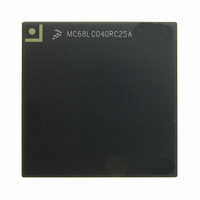
MC68LC040RC25A Freescale Semiconductor, MC68LC040RC25A Datasheet - Page 98

MC68LC040RC25A
Manufacturer Part Number
MC68LC040RC25A
Description
IC MPU 32BIT 25MHZ 179-PGA
Manufacturer
Freescale Semiconductor
Datasheet
1.MC68EC040FE33A.pdf
(442 pages)
Specifications of MC68LC040RC25A
Processor Type
M680x0 32-Bit
Speed
25MHz
Voltage
5V
Mounting Type
Surface Mount
Package / Case
179-PGA
Lead Free Status / RoHS Status
Lead free / RoHS Compliant
Features
-
Available stocks
Company
Part Number
Manufacturer
Quantity
Price
Company:
Part Number:
MC68LC040RC25A
Manufacturer:
MOT
Quantity:
6 100
Company:
Part Number:
MC68LC040RC25A
Manufacturer:
Freescale Semiconductor
Quantity:
135
- Current page: 98 of 442
- Download datasheet (4Mb)
Freescale Semiconductor, Inc.
4.7.1 Instruction Cache
The IU uses the instruction cache to store instruction prefetches as it requests them.
Instruction prefetches are normally requested from sequential memory locations except
when a change of program flow occurs (e.g., a branch taken) or when an instruction that
can modify the status register (SR) is executed, in which case the instruction pipe is
automatically flushed and refilled. The instruction cache supports a line-based protocol
that allows individual cache lines to be in either the invalid or valid states.
For instruction prefetch requests that hit in the cache, the half-line selected by physical
address bit 3 is multiplexed onto the internal instruction data bus. When an access misses
in the cache, the cache controller requests the line containing the required data from
memory and places it in the cache. If available, an invalid line is selected and updated
with the tag and data from memory. The line state then changes from invalid to valid by
setting the V-bit. If all lines in the set are already valid, a pseudo-random replacement
algorithm is used to select one of the four cache lines replacing the tag and data contents
of the line with the new line information. Figure 4-5 illustrates the instruction-cache line
state transitions resulting from processor and snoop controller accesses. Transitions are
labeled with a capital letter, indicating the previous state, followed by a number indicating
the specific case listed in Table 4-3.
I3–CINV/CPUSH
V1–CPU READ MISS
V2–CPU READ HIT
I1-CPU READ MISS
INVALID
VALID
V3–CINV/CPUSH
V5–SNOOP READ HIT
V6–SNOOP WRITE HIT
Figure 4-5. Instruction-Cache Line State Diagram
4-14
M68040 USER'S MANUAL
MOTOROLA
For More Information On This Product,
Go to: www.freescale.com
Related parts for MC68LC040RC25A
Image
Part Number
Description
Manufacturer
Datasheet
Request
R
Part Number:
Description:
Manufacturer:
Freescale Semiconductor, Inc
Datasheet:
Part Number:
Description:
Manufacturer:
Freescale Semiconductor, Inc
Datasheet:
Part Number:
Description:
Manufacturer:
Freescale Semiconductor, Inc
Datasheet:
Part Number:
Description:
Manufacturer:
Freescale Semiconductor, Inc
Datasheet:
Part Number:
Description:
Manufacturer:
Freescale Semiconductor, Inc
Datasheet:
Part Number:
Description:
Manufacturer:
Freescale Semiconductor, Inc
Datasheet:
Part Number:
Description:
Manufacturer:
Freescale Semiconductor, Inc
Datasheet:
Part Number:
Description:
Manufacturer:
Freescale Semiconductor, Inc
Datasheet:
Part Number:
Description:
Manufacturer:
Freescale Semiconductor, Inc
Datasheet:
Part Number:
Description:
Manufacturer:
Freescale Semiconductor, Inc
Datasheet:
Part Number:
Description:
Manufacturer:
Freescale Semiconductor, Inc
Datasheet:
Part Number:
Description:
Manufacturer:
Freescale Semiconductor, Inc
Datasheet:
Part Number:
Description:
Manufacturer:
Freescale Semiconductor, Inc
Datasheet:
Part Number:
Description:
Manufacturer:
Freescale Semiconductor, Inc
Datasheet:
Part Number:
Description:
Manufacturer:
Freescale Semiconductor, Inc
Datasheet:


