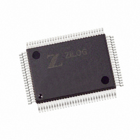
Z8018110FEG Zilog, Z8018110FEG Datasheet - Page 6

Z8018110FEG
Manufacturer Part Number
Z8018110FEG
Description
IC 10MHZ ACCESS CTRL 100-QFP
Manufacturer
Zilog
Datasheet
1.Z8018110FEG.pdf
(74 pages)
Specifications of Z8018110FEG
Processor Type
Z180
Features
Smart Access Controller SAC™
Speed
10MHz
Voltage
5V
Mounting Type
Surface Mount
Package / Case
100-QFP
Processor Series
Z8018xx
Core
Z80
Data Bus Width
8 bit
Program Memory Type
ROMLess
Program Memory Size
1 MB
Interface Type
ASCI, UART
Maximum Clock Frequency
10 MHz
Number Of Programmable I/os
16
Number Of Timers
2
Operating Supply Voltage
4.5 V to 5.5 V
Maximum Operating Temperature
+ 100 C
Mounting Style
SMD/SMT
Development Tools By Supplier
Z8018100ZCO
Minimum Operating Temperature
- 40 C
Lead Free Status / RoHS Status
Lead free / RoHS Compliant
Other names
269-4692
Z8018110FEG
Z8018110FEG
Available stocks
Company
Part Number
Manufacturer
Quantity
Price
Company:
Part Number:
Z8018110FEG
Manufacturer:
Zilog
Quantity:
340
Part Number:
Z8018110FEG
Manufacturer:
ZELOG
Quantity:
20 000
Zilog
PERIPHERAL SIGNALS
Pin Name
RXA0, RXA1
TXA0, TXA1
/RTS0
/DCD0
/CTS0
/CTS1/RXS
CKA0//DREQ0
CKA1//TEND0
/TEND1
CKS
TXS
/DREQ1
2-6
Pin Number
70, 74
69, 72
66
68
67
77
71
75
80
78
76
79
Input/Output, Tri-State
In, Active 1
Out, Active 1
Out, Active 0
In, Active 0
In, Active 0
In, Active 0
I/O, Active 1
I/O, Active 1
Out, Active 0
I/O, Active 1
Out, Active 1
In, Active 0
PS009701-0301
Function
ASCI Receive Data 0 and 1. These signals are the receive
data to the ASCI channels.
ASCI Transmit Data 0 and 1. These signals are the
receive data to the ASCI channels. Transmit data changes
are with respect to the falling edge of the transmit clock.
Request to Send 0. This is a programmable modem
control signal for ASCI channel 0.
Data Carrier Detect 0. This is a programmable modem
control signal for ASCI channel 0.
Clear To Send 0. This is a programmable modem control
signal for ASCI channel 0.
Clear To Send 0/Clocked Serial Receive Data. This is a
programmable modem control signal for ASCI channel 0.
Also, this signal becomes receive data for the CSIO
channel under program control. On power-on Reset, this
pin is set as RxS.
Asynchronous Clock0/DMAC0 Request. This pin is the
transmit and receive clock for the Asynchronous channel
0. Also, under program control, this pin is used to request
a DMA transfer from DMA channel 0. DMA0 monitors this
input to determine when an external device is ready for a
read or write operation. On power-on Reset, this pin is
initialized as CKA0.
Asynchronous Clock1/DMAC0 Transfer End. This pin is
the transmit and receive clock for the Asynchronous chan-
nel 1. Also, under program control, this pin becomes
/TEND0 and is asserted during the last write cycle of the
DMA0 operation and is used to indicate the end of the
block transfer. On power-on Reset, this pin initializes
as CKA1.
DMAC1 Transfer End. This pin is asserted during the last
write cycle of the DMA1 operation and is used to indicate
the end of the block transfer.
CSIO Clock. This line is the clock for the CSIO channel.
CSI/O Tx Data. This line carries the transmit data from the
CSIO channel.
DMAC1 Request. This pin is used to request a DMA
transfer from DMA channel 1. DMA1 monitors this input to
determine when an external device is ready for a read or
write operation.
S
MART
A
CCESS
C
DS971800500
ONTROLLER
Z80181
SAC
™


