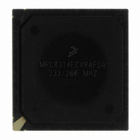
MPC8314ECVRAFDA Freescale Semiconductor, MPC8314ECVRAFDA Datasheet - Page 103

MPC8314ECVRAFDA
Manufacturer Part Number
MPC8314ECVRAFDA
Description
MPU POWERQUICC II PRO 620-PBGA
Manufacturer
Freescale Semiconductor
Datasheet
1.MPC8314VRADDA.pdf
(106 pages)
Specifications of MPC8314ECVRAFDA
Processor Type
MPC83xx PowerQUICC II Pro 32-Bit
Speed
333MHz
Voltage
1V
Mounting Type
Surface Mount
Package / Case
620-PBGA
Processor Series
MPC8xxx
Core
e300
Data Bus Width
32 bit
Maximum Clock Frequency
50 MHz
Maximum Operating Temperature
+ 105 C
Mounting Style
SMD/SMT
Minimum Operating Temperature
- 40 C
Lead Free Status / RoHS Status
Lead free / RoHS Compliant
Features
-
Lead Free Status / Rohs Status
Lead free / RoHS Compliant
Available stocks
Company
Part Number
Manufacturer
Quantity
Price
Company:
Part Number:
MPC8314ECVRAFDA
Manufacturer:
Freescale Semiconductor
Quantity:
135
Company:
Part Number:
MPC8314ECVRAFDA
Manufacturer:
Freescale Semiconductor
Quantity:
10 000
25.4
To ensure reliable operation, it is highly recommended to connect unused inputs to an appropriate signal
level. Unused active low inputs should be tied to NVDD, GVDD, or LVDD as required. Unused active
high inputs should be connected to GND. All NC (no-connect) signals must remain unconnected.
Power and ground connections must be made to all external VDD, GVDD, LVDD, NVDD, and GND pins
of the device.
25.5
The MPC8314E drivers are characterized over process, voltage, and temperature. For all buses, the driver
is a push-pull single-ended driver type (open drain for I
To measure Z
or GND. Then, the value of each resistor is varied until the pad voltage is NVDD/2 (see
output impedance is the average of two components, the resistances of the pull-up and pull-down devices.
When data is held high, SW1 is closed (SW2 is open) and R
NVDD/2. R
each other in value. Then, Z
The value of this resistance and the strength of the driver’s current source can be found by making two
measurements. First, the output voltage is measured while driving logic 1 without an external differential
termination resistor. The measured voltage is V
while driving logic 1 with an external precision differential termination resistor of value R
measured voltage is V
R
Table 76
nominal NVDD, 105°C.
Freescale Semiconductor
term
× (V
summarizes the signal impedance targets. The driver impedance are targeted at minimum VDD,
Connection Recommendations
Output Buffer DC Impedance
1
/V
P
0
then becomes the resistance of the pull-up devices. R
2
for the single-ended drivers, an external resistor is connected from the chip pad to NVDD
– 1). The drive current is then I
MPC8314E PowerQUICC
2
= (1/(1/R
0
= (R
Figure 62. Driver Impedance Measurement
1
Data
P
+ 1/R
+ R
N
2
™
)/2.
)) × I
II Pro Processor Hardware Specifications, Rev. 0
1
source
source
= R
source
. Solving for the output impedance gives R
= V
2
C).
1
× I
/R
Pad
P
R
source
R
source
is trimmed until the voltage at the pad equals
NVDD
OGND
N
P
. Second, the output voltage is measured
.
P
SW2
SW1
and R
N
are designed to be close to
System Design Information
Figure
term
. The
source
62). The
=
103


