MPC8314ECVRAFDA Freescale Semiconductor, MPC8314ECVRAFDA Datasheet - Page 48
MPC8314ECVRAFDA
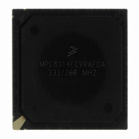
Manufacturer Part Number
MPC8314ECVRAFDA
Description
MPU POWERQUICC II PRO 620-PBGA
Manufacturer
Freescale Semiconductor
Datasheet
1.MPC8314VRADDA.pdf
(106 pages)
Specifications of MPC8314ECVRAFDA
Processor Type
MPC83xx PowerQUICC II Pro 32-Bit
Speed
333MHz
Voltage
1V
Mounting Type
Surface Mount
Package / Case
620-PBGA
Processor Series
MPC8xxx
Core
e300
Data Bus Width
32 bit
Maximum Clock Frequency
50 MHz
Maximum Operating Temperature
+ 105 C
Mounting Style
SMD/SMT
Minimum Operating Temperature
- 40 C
Lead Free Status / RoHS Status
Lead free / RoHS Compliant
Features
-
Lead Free Status / Rohs Status
Lead free / RoHS Compliant
Available stocks
Company
Part Number
Manufacturer
Quantity
Price
Company:

Part Number:
MPC8314ECVRAFDA
Manufacturer:
Freescale Semiconductor
Quantity:
135
Company:
Part Number:
MPC8314ECVRAFDA
Manufacturer:
Freescale Semiconductor
Quantity:
10 000


PCI
Figure 32
Figure 33
14 PCI
This section describes the DC and AC electrical specifications for the PCI bus of the MPC8314E.
48
All values refer to V
Noise margin at the HIGH level for each connected device (including hysteresis)
Notes:
1. The symbols used for timing specifications follow the pattern of t
2. MPC8314E provides a hold time of at least 300 ns for the SDA signal (referred to the V
3. The maximum t
4. MPC8314E does not follow the I2C-BUS Specifications version 2.1 regarding the tI2CF AC parameter.
inputs and t
(I2) with respect to the time data input signals (D) reach the valid state (V) relative to the t
the high (H) state or setup time. Also, t
condition (S) went invalid (X) relative to the t
symbolizes I
to the t
with the appropriate letter: R (rise) or F (fall).
undefined region of the falling edge of SCL.
SDA
SCL
I2C
provides the AC test load for the I
shows the AC timing diagram for the I
clock reference (K) going to the high (H) state or setup time. For rise and fall times, the latter convention is used
S
(first two letters of functional block)(reference)(state)(signal)(state)
2
IH
C timing (I2) for the time that the data with respect to the stop condition (P) reaching the valid state (V) relative
(min) and V
I2DVKH
t
I2CF
t
I2CL
t
MPC8314E PowerQUICC
I2SXKL
has to be met only if the device does not stretch the LOW period (t
Output
IL
Table 48. I
(max) levels (see
Parameter
Figure 33. I
t
I2SXKL
I2DXKL
2
C AC Electrical Specifications (continued)
Figure 32. I
Table
I2C
Z
t
™
symbolizes I
I2DVKH
0
II Pro Processor Hardware Specifications, Rev. 0
clock reference (K) going to the low (L) state or hold time. Also, t
= 50 Ω
t
47)
I2CH
2
2
C.
C Bus AC Timing Diagram
t
2
I2SXKL
2
C bus.
C AC Test Load
2
C timing (I2) for the time that the data with respect to the start
(first two letters of functional block)(signal)(state)(reference)(state)
Sr
for outputs. For example, t
t
I2SVKH
t
I2KHKL
R
L
= 50 Ω
Symbol
V
NH
t
IHmin
I2PVKH
1
NVDD/2
I2CL
I2C
0.2 × NVDD
of the SCL signal) to bridge the
t
I2DVKH
I2CR
clock reference (K) going to
) of the SCL signal.
Min
Freescale Semiconductor
symbolizes I
P
t
I2CF
Max
—
S
2
C timing
I2PVKH
Unit
for
V
Related parts for MPC8314ECVRAFDA
Image
Part Number
Description
Manufacturer
Datasheet
Request
R

Part Number:
Description:
Powerquicc Ii Pro Processor Hardware Specifications
Manufacturer:
Freescale Semiconductor, Inc
Datasheet:
Part Number:
Description:
Manufacturer:
Freescale Semiconductor, Inc
Datasheet:
Part Number:
Description:
Manufacturer:
Freescale Semiconductor, Inc
Datasheet:
Part Number:
Description:
Manufacturer:
Freescale Semiconductor, Inc
Datasheet:
Part Number:
Description:
Manufacturer:
Freescale Semiconductor, Inc
Datasheet:
Part Number:
Description:
Manufacturer:
Freescale Semiconductor, Inc
Datasheet:
Part Number:
Description:
Manufacturer:
Freescale Semiconductor, Inc
Datasheet:
Part Number:
Description:
Manufacturer:
Freescale Semiconductor, Inc
Datasheet:
Part Number:
Description:
Manufacturer:
Freescale Semiconductor, Inc
Datasheet:
Part Number:
Description:
Manufacturer:
Freescale Semiconductor, Inc
Datasheet:
Part Number:
Description:
Manufacturer:
Freescale Semiconductor, Inc
Datasheet:
Part Number:
Description:
Manufacturer:
Freescale Semiconductor, Inc
Datasheet:
Part Number:
Description:
Manufacturer:
Freescale Semiconductor, Inc
Datasheet:
Part Number:
Description:
Manufacturer:
Freescale Semiconductor, Inc
Datasheet:
Part Number:
Description:
Manufacturer:
Freescale Semiconductor, Inc
Datasheet: