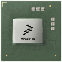
MPC8541EVTAQF Freescale Semiconductor, MPC8541EVTAQF Datasheet - Page 62

MPC8541EVTAQF
Manufacturer Part Number
MPC8541EVTAQF
Description
IC MPU POWERQUICC III 783-FCPBGA
Manufacturer
Freescale Semiconductor
Datasheet
1.MPC8541EVTALF.pdf
(88 pages)
Specifications of MPC8541EVTAQF
Processor Type
MPC85xx PowerQUICC III 32-Bit
Speed
1.0GHz
Voltage
1.3V
Mounting Type
Surface Mount
Package / Case
783-FCPBGA
Processor Series
MPC85xx
Core
e500
Data Bus Width
32 bit
Development Tools By Supplier
RDK-IDM-SBC
Maximum Clock Frequency
1000 MHz
Maximum Operating Temperature
+ 105 C
Mounting Style
SMD/SMT
I/o Voltage
2.5 V, 3.3 V
Minimum Operating Temperature
0 C
For Use With
MPC8548CDS - DEV TOOLS CDS FOR 8548CWH-PPC-8540N-VE - KIT EVAL SYSTEM MPC8540
Lead Free Status / RoHS Status
Lead free / RoHS Compliant
Features
-
Lead Free Status / Rohs Status
Lead free / RoHS Compliant
Available stocks
Company
Part Number
Manufacturer
Quantity
Price
Company:
Part Number:
MPC8541EVTAQF
Manufacturer:
Freescale Semiconductor
Quantity:
10 000
Package and Pin Listings
62
GND
GV
LV
MV
No Connects
OV
RESERVED
SENSEVDD
SENSEVSS
V
PA[8:31]
DD
DD
DD
DD
REF
MPC8541E PowerQUICC™ III Integrated Communications Processor Hardware Specification, Rev. 4.2
Signal
A12, A17, B3, B14, B20, B26, B27, C2, C4, C11,C17,
C19, C22, C27, D8, E3, E12, E24, F11, F18, F23, G9,
V10, V26, W5, W18, W23, Y8, Y16, AA6, AA13, AB4,
AB11, AB19, AC6, AC9, AD3, AD8, AD17, AF2, AF4,
F19, F25, G13, G18, G20, G23, G28, H19, H24, J12,
D1, E4, H3, K4, K10, L7, M5, N3, P22, R19, R25, T2,
T7, U5, U20, U26, V8, W4, W13, W19, W21, Y7, Y23,
M13, M15, M17, N14, N16, P13, P15, P17, R12, R14,
J7, J8, K8, K7, K6, K3, K2, K1, L1, L2, L3, L4, L5, L8,
M14, M16, M22, M27, N2, N13, N15, N17, P12, P14,
C28, D16, D19, D21, D24, D28, E17, E22, F12, F15,
J24, K5, K9, K18, K23, K28, L6, L20, L25, M4, M12,
A14, A20, A25, A26, A27, A28, B17, B22, B28, C12,
AE25, AE26, AE27, AF24, AF25, H1, H2, J1, J2, J3,
G12, G25, H4, H12, H14, H17, H20, H22, H27, J19,
J17, J22, J27, K15, K20, K25, L13, L23, L28, M25,
V25, W24, W25, W9, Y24, Y25, Y5, Y6, Y9, AH26,
J4, J5, J6, M1, N1, N10, N11, N4, N5, N7, N8, N9,
T12, T14, T16, U6, U13, U15, U16, U17, U21, V7,
P16, P23, R13, R15, R17, R20, R26, T3, T8, T10,
P10, P8, P9, R10, R11, T24, T25, U24, U25, V24,
AA5, AA12, AA16, AA20, AB7, AB9, AB26, AC5,
AC11, AC17, AD4, AE1, AE8, AE10, AE15, AF7,
AA24, AA25, AA3, AA4, AA7 AA8, AB24, AB25,
AC24, AC25, AD23, AD24, AD25, AE23, AE24,
Table 43. MPC8541E Pinout Listing (continued)
AH28, AG28, AH1, AG1, AH2, B1, B2, A2, A3
L9, L10, L11, M10, M9, M8, M7, M6, M3, M2
AF10, AF13, AF15, AF27, AG3, AG7
R16, T13, T15, T17, U12, U14
Package Pin Number
C1, T11, U11, AF1
AF12, AG27, AH4
A4, C5, E7, H10
N21
N27
K12
L12
CPM
Power for DDR
Voltage Signal;
other Standard
Power for Core
Power for Core
Ethernet, and
Three-Speed
(2.5 V, 3.3 V)
Ethernet I/O
PCI, 10/100
Reference
Reference
DRAM I/O
Pin Type
Voltage;
Voltage
(2.5 V)
(3.3 V)
(1.2 V)
(1.2 V)
DDR
—
—
—
—
I/0
Freescale Semiconductor
Supply
MV
Power
GV
OV
OV
LV
V
V
—
—
—
—
DD
DD
DD
REF
DD
DD
DD
Notes
16
15
13
13
—
—
—
—
—
—
—


