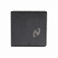
DP8344BV National Semiconductor, DP8344BV Datasheet - Page 140

DP8344BV
Manufacturer Part Number
DP8344BV
Description
IC BIPHASE COMM PROCESSR 84-PLCC
Manufacturer
National Semiconductor
Datasheet
1.DP8344BV.pdf
(184 pages)
Specifications of DP8344BV
Processor Type
8-Bit RISC
Speed
20MHz
Voltage
4.5 ~ 5.5V
Mounting Type
Surface Mount
Package / Case
84-PLCC
Operating Supply Voltage (typ)
5V
Operating Supply Voltage (max)
5.5V
Operating Supply Voltage (min)
4.5V
Mounting
Surface Mount
Operating Temperature (max)
70C
Operating Temperature (min)
0C
Operating Temperature Classification
Commercial
Lead Free Status / RoHS Status
Contains lead / RoHS non-compliant
Features
-
Lead Free Status / Rohs Status
Not Compliant
Other names
*DP8344BV
Available stocks
Company
Part Number
Manufacturer
Quantity
Price
Company:
Part Number:
DP8344BV
Manufacturer:
NSC
Quantity:
5 510
Part Number:
DP8344BV
Manufacturer:
NS/国半
Quantity:
20 000
- Current page: 140 of 184
- Download datasheet (3Mb)
Figure 6-1
6 0 Reference Section
CPL Complement
Syntax
CPL Rsd
Affected Flags
N Z
Description
Logically complements the contents of the register Rsd
placing the result back into that register
Example
Load the fill-bit count passed from the host into the Trans-
mitter’s Fill-Bit Register FBR
required one’s complement of the fill-bit count In this exam-
ple register 20 contains the fill-bit count
Instruction Format
T-states
2
Bus Timing
Operation
Rsd
1
15
EXX
MOVE
CPL
0
Rsd
1
0
1 1
R20 FBR
FBR
1
Opcode
register
1
1
select alternate banks
complement fill-bit count
load FBR
0
0
R3 and then perform the
0
(Continued)
0
4
Rsd
0
140
Figure 6-1
EXX Exchange Register Banks
Syntax
EXX ba bb
Affected Flags
None
Description
Selects which CPU register banks are active by exchanging
between the main and alternate register sets for each bank
Bank A controls R0– R3 and Bank B controls R4– R11 The
table below shows the four possible register bank configura-
tions Note that deactivated registers retain their current val-
ues The Global Interrupt Enable bit GIE can be set or
cleared if desired
Example
Activate the main register set of Bank A the alternate regis-
ter set of Bank B and leave the Global Interrupt Enable bit
Instruction Format
T-states
2
Bus Timing
Operation
Case ba of
End case
Case bb of
End case
Case g of
End case
GIE unchanged
1 0 1 0 1 1 1 0 1
15
EXX
0
1
0
1
0
1
2
3
activate main Bank A
activate alternate Bank A
activate main Bank B
activate alternate Bank B
leave GIE unaffected (default)
(reserved)
set GIE
clear GIE
ba
0
0
1
1
0 1
Opcode
Register Bank Configurations
g
bb
0
1
0
1
select main A alt B reg banks
Active Register Banks
Main A Main B
Main A Alternate B
Alternate A Main B
Alternate A Alternate B
6
00 GIE not affected
01 reserved
10 Set GIE
11 Clear GIE
g
ba bb
4
3
0 0 0
2
0
Related parts for DP8344BV
Image
Part Number
Description
Manufacturer
Datasheet
Request
R

Part Number:
Description:
Biphase Communications Processor?BCP
Manufacturer:
NSC [National Semiconductor]
Datasheet:
Part Number:
Description:
National Semiconductor [8-Bit D/A Converter]
Manufacturer:
National Semiconductor
Datasheet:
Part Number:
Description:
National Semiconductor [Media Coprocessor]
Manufacturer:
National Semiconductor
Datasheet:
Part Number:
Description:
Digitally Controlled Tone and Volume Circuit with Stereo Audio Power Amplifier, Microphone Preamp Stage and National 3D Sound
Manufacturer:
National Semiconductor
Datasheet:
Part Number:
Description:
Digitally Controlled Tone and Volume Circuit with Stereo Audio Power Amplifier, Microphone Preamp Stage and National 3D Sound
Manufacturer:
National Semiconductor
Datasheet:
Part Number:
Description:
AC97 Rev 2 Codec with Sample Rate Conversion and National 3D Sound
Manufacturer:
National Semiconductor
Part Number:
Description:
Manufacturer:
National Semiconductor
Datasheet:
Part Number:
Description:
Manufacturer:
National Semiconductor
Datasheet:
Part Number:
Description:
General Purpose, Low Voltage, Low Power, Rail-to-Rail Output Operational Amplifiers
Manufacturer:
National Semiconductor
Datasheet:
Part Number:
Description:
8-bit 20 MSPS flash A/D converter.
Manufacturer:
National Semiconductor
Datasheet:
Part Number:
Description:
Low Noise Quad Operational Amplifier
Manufacturer:
National Semiconductor
Datasheet:
Part Number:
Description:
Quad Differential Line Receivers
Manufacturer:
National Semiconductor
Datasheet:
Part Number:
Description:
Quad High Speed Trapezoidal? Bus Transceiver
Manufacturer:
National Semiconductor
Datasheet:
Part Number:
Description:
Dual Line Receiver
Manufacturer:
National Semiconductor
Datasheet:


