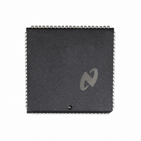
DP8344BV National Semiconductor, DP8344BV Datasheet - Page 39

DP8344BV
Manufacturer Part Number
DP8344BV
Description
IC BIPHASE COMM PROCESSR 84-PLCC
Manufacturer
National Semiconductor
Datasheet
1.DP8344BV.pdf
(184 pages)
Specifications of DP8344BV
Processor Type
8-Bit RISC
Speed
20MHz
Voltage
4.5 ~ 5.5V
Mounting Type
Surface Mount
Package / Case
84-PLCC
Operating Supply Voltage (typ)
5V
Operating Supply Voltage (max)
5.5V
Operating Supply Voltage (min)
4.5V
Mounting
Surface Mount
Operating Temperature (max)
70C
Operating Temperature (min)
0C
Operating Temperature Classification
Commercial
Lead Free Status / RoHS Status
Contains lead / RoHS non-compliant
Features
-
Lead Free Status / Rohs Status
Not Compliant
Other names
*DP8344BV
Available stocks
Company
Part Number
Manufacturer
Quantity
Price
Company:
Part Number:
DP8344BV
Manufacturer:
NSC
Quantity:
5 510
Part Number:
DP8344BV
Manufacturer:
NS/国半
Quantity:
20 000
- Current page: 39 of 184
- Download datasheet (3Mb)
2 0 CPU Description
LOCK is another input which affects BCP instruction timing
LOCK prevents the BCP from accessing data memory
When asserted low LOCK will cause the BCP to wait when
it executes a data memory access instruction The BCP will
be waited until LOCK is taken high To prevent a given ac-
cess of data memory LOCK must be asserted low one-half
T-state prior to the beginning of the instruction accessing
data memory Figure 2-30 shows LOCK being used to wait a
write to data memory LOCK falls prior to the falling edge of
CPU-CLK before T1 In order to guarantee at least one wait
state LOCK is held low until after the falling edge of CPU-
CLK in T1 This causes the insertion of TW into the cycle
prior to TX ALE remains high and the address is delayed on
AD until LOCK is removed After LOCK rises the access
concludes normally with ALE falling halfway through TX and
WRITE occurring during T2 Note that LOCK waits the ac-
cess at a different point in the cycle than programmed wait
FIGURE 2-28 Three T-state Program Control Instruction WAIT Timing
FIGURE 2-29 Four T-state Program Control Instruction WAIT Timing
(Continued)
39
states or WAIT Additional wait states could occur from
these sources prior to T2 Figure 2-31 shows an example of
LOCK holding off a write to data memory with one pro-
grammed wait state
With timing similar to LOCK the BCP will be delayed from
making a data memory access by an access from the re-
mote system If the remote system is accessing the Remote
Interface Configuration register
BCP will be waited by the Remote Interface and Arbitration
System RIAS until the remote access is finished The
length of time the BCP is waited depends on the speed of
the remote system and the type of remote access The wait
states are added prior to TX in the same manner as for
LOCK shown in Figure 2-30 A more detailed description of
the operation of RIAS can be found in Section 4 0 Remote
Interface and Arbitration System
RIC
or data memory the
TL F 9336 – F1
TL F 9336 – F2
Related parts for DP8344BV
Image
Part Number
Description
Manufacturer
Datasheet
Request
R

Part Number:
Description:
Biphase Communications Processor?BCP
Manufacturer:
NSC [National Semiconductor]
Datasheet:
Part Number:
Description:
National Semiconductor [8-Bit D/A Converter]
Manufacturer:
National Semiconductor
Datasheet:
Part Number:
Description:
National Semiconductor [Media Coprocessor]
Manufacturer:
National Semiconductor
Datasheet:
Part Number:
Description:
Digitally Controlled Tone and Volume Circuit with Stereo Audio Power Amplifier, Microphone Preamp Stage and National 3D Sound
Manufacturer:
National Semiconductor
Datasheet:
Part Number:
Description:
Digitally Controlled Tone and Volume Circuit with Stereo Audio Power Amplifier, Microphone Preamp Stage and National 3D Sound
Manufacturer:
National Semiconductor
Datasheet:
Part Number:
Description:
AC97 Rev 2 Codec with Sample Rate Conversion and National 3D Sound
Manufacturer:
National Semiconductor
Part Number:
Description:
Manufacturer:
National Semiconductor
Datasheet:
Part Number:
Description:
Manufacturer:
National Semiconductor
Datasheet:
Part Number:
Description:
General Purpose, Low Voltage, Low Power, Rail-to-Rail Output Operational Amplifiers
Manufacturer:
National Semiconductor
Datasheet:
Part Number:
Description:
8-bit 20 MSPS flash A/D converter.
Manufacturer:
National Semiconductor
Datasheet:
Part Number:
Description:
Low Noise Quad Operational Amplifier
Manufacturer:
National Semiconductor
Datasheet:
Part Number:
Description:
Quad Differential Line Receivers
Manufacturer:
National Semiconductor
Datasheet:
Part Number:
Description:
Quad High Speed Trapezoidal? Bus Transceiver
Manufacturer:
National Semiconductor
Datasheet:
Part Number:
Description:
Dual Line Receiver
Manufacturer:
National Semiconductor
Datasheet:


