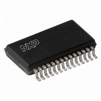
UDA1345TS/N2,112 NXP Semiconductors, UDA1345TS/N2,112 Datasheet - Page 23

UDA1345TS/N2,112
Manufacturer Part Number
UDA1345TS/N2,112
Description
IC AUDIO CODEC 28-SSOP
Manufacturer
NXP Semiconductors
Type
Stereo Audior
Datasheet
1.UDA1345TSN2118.pdf
(29 pages)
Specifications of UDA1345TS/N2,112
Package / Case
28-SSOP (0.200", 5.30mm Width)
Data Interface
Serial
Resolution (bits)
24 b
Number Of Adcs / Dacs
2 / 2
Sigma Delta
Yes
S/n Ratio, Adcs / Dacs (db) Typ
94 / 98
Voltage - Supply, Analog
2.4 V ~ 3.6 V
Voltage - Supply, Digital
2.4 V ~ 3.6 V
Operating Temperature
-40°C ~ 85°C
Mounting Type
Surface Mount
Number Of Adc Inputs
2
Number Of Dac Outputs
2
Conversion Rate
100 KSPS
Interface Type
Serial (I2S) or L3
Resolution
24 bit
Operating Supply Voltage
2.4 V to 3.6 V
Maximum Operating Temperature
+ 85 C
Mounting Style
SMD/SMT
Minimum Operating Temperature
- 40 C
Number Of Channels
2 ADC / 2 DAC
Supply Current
10 mA
Lead Free Status / RoHS Status
Lead free / RoHS Compliant
Lead Free Status / RoHS Status
Lead free / RoHS Compliant, Lead free / RoHS Compliant
Other names
568-1157-5
935266777112
UDA1345TSDB
935266777112
UDA1345TSDB
Available stocks
Company
Part Number
Manufacturer
Quantity
Price
Company:
Part Number:
UDA1345TS/N2,112
Manufacturer:
ON
Quantity:
12 000
NXP Semiconductors
13 APPLICATION INFORMATION
The application information as given in Fig.9 is an optimum application environment. Simplification is possible at the cost
of some performance degradation. The following notes apply:
• The capacitors at the output of the DAC can be reduced. It should be noted that the cut-off frequency of the DC filter
• The capacitors at the input of the ADC can also be reduced. It should be noted that the cut-off frequency of the
2002 May 28
also changes.
capacitor with the 12 kW input resistance of the ADC will also change.
Economy audio CODEC
ground
overload
system
clock
input
input
right
flag
left
3 V
X4
X5
8LM32A07
8LM32A07
L1
L2
(16 V)
(16 V)
47 μF
47 μF
C1
C6
47 Ω
100 μF
R30
(16 V)
C12
100 μF
(16 V)
C11
V DDA
V DDD
SYSCLK
DATAO
DATAI
VINR
VINL
MP1
MP2
MP3
MP4
BCK
WS
12
18
16
17
19
9
3
5
13
14
15
1
V SSA(ADC)
100 μF
100 nF
(16 V)
(63 V)
C21
C2
Fig.9 Application diagram.
V SSO
27
100 μF
100 nF
2
(16 V)
(63 V)
C26
V DDA(ADC) V ADCN
V DDA
C7
R21
1 Ω
V DDO
25
UDA1345TS
V DDO
10 Ω
R25
1 Ω
23
R24
6
100 nF
(63 V)
C25
22
V SSA(DAC)
7
V ADCP
100 nF
100 μF
(63 V)
(16 V)
C27
C10
11
V DDA
V SSD
23
V DDA(DAC)
R29
1 Ω
V DDD
10
V DDD
R28
10 Ω
26
24
28
4
V ref(A)
VOUTL
VOUTR
V ref(D)
(16 V)
(16 V)
47 μF
47 μF
C5
C8
C23
100 nF
(63 V)
C22
100 nF
(63 V)
R22
10 kΩ
R27
10 kΩ
UDA1345TS
Product specification
100 Ω
100 Ω
C3
47 μF
(16 V)
R26
R23
C4
47 μF
(16 V)
X2
X3
MGS877
output
output
right
left


