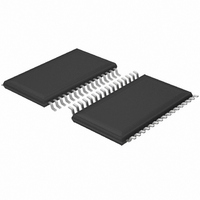
UDA1380TT/N2,518 NXP Semiconductors, UDA1380TT/N2,518 Datasheet - Page 26

UDA1380TT/N2,518
Manufacturer Part Number
UDA1380TT/N2,518
Description
IC AUDIO CODER-DECODER 32-TSSOP
Manufacturer
NXP Semiconductors
Type
Stereo Audior
Datasheet
1.UDA1380HNN2118.pdf
(68 pages)
Specifications of UDA1380TT/N2,518
Data Interface
I²C, Serial
Resolution (bits)
24 b
Number Of Adcs / Dacs
2 / 2
Sigma Delta
No
S/n Ratio, Adcs / Dacs (db) Typ
97 / 100
Voltage - Supply, Analog
2.4 V ~ 3.6 V
Voltage - Supply, Digital
2.4 V ~ 3.6 V
Operating Temperature
-40°C ~ 85°C
Mounting Type
Surface Mount
Package / Case
32-TSSOP
Lead Free Status / RoHS Status
Lead free / RoHS Compliant
Other names
935270659518
UDA1380TT-T
UDA1380TT-T
UDA1380TT-T
UDA1380TT-T
NXP Semiconductors
10 I
The UDA1380 supports I
mode as well as the L3-bus mode; all features can be
controlled by the microcontroller with the same register
addresses as in the L3-bus mode.
The exchange of data and control information between the
microcontroller and the UDA1380 in I
accomplished through a serial hardware interface
comprising the following pins:
Figure 20 shows the clock and data timing of the I
transfer.
10.1
Before any data is transmitted on the I
which should respond is addressed first. The addressing is
always done with the first byte transmitted after the start
procedure. The UDA1380 device address is
[A6 to A0] 00110(A1)0, with bit A1 as the address
selection bit (two addresses possible).
2004 Apr 22
L3CLOCK/SCL: microcontroller interface clock line,
SCL
L3MODE: sets the bit A1of the I
L3DATA/SDA: microcontroller interface data line, SDA.
Stereo audio coder-decoder
for MD, CD and MP3
2
C-BUS INTERFACE DESCRIPTION
Addressing
2
C-bus microcontroller interface
2
C-bus device address
2
C-bus mode is
2
C-bus, the device
2
C-bus
26
10.1.1
The UDA1380 acts as either a slave receiver or a slave
transmitter. Therefore the clock signal SCL is only an input
signal. The data signal SDA is a bidirectional line. Table 11
shows the device address of the UDA1380.
The device can be set to one of the two addresses by using
bit A1 (which is pin L3MODE) to select.
Table 11 I
10.1.2
Table 12 shows the register address format of the
UDA1380. The register mapping in I
same as for the L3-bus interface.
Table 12 I
(MSB)
(MSB)
0
0
D
R
2
2
EVICE ADDRESS
EGISTER ADDRESS
A6
C-bus device address
C-bus register address
0
A5
1
A4
1
(
PIN
BIT
BIT
A1)
A3
0
2
Product specification
C-bus mode is the
A1
A2
UDA1380
A1
0
(LSB)
(LSB)
R/W
A0


