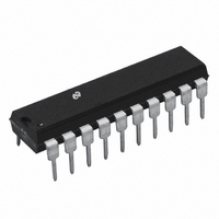
TP3064J National Semiconductor, TP3064J Datasheet - Page 4

TP3064J
Manufacturer Part Number
TP3064J
Description
IC FILTER MONO SRL COMBO 20DIP
Manufacturer
National Semiconductor
Type
PCM Codec/Filterr
Datasheet
1.TP3067VNOPB.pdf
(18 pages)
Specifications of TP3064J
Data Interface
Serial
Resolution (bits)
8 b
Number Of Adcs / Dacs
1 / 1
Sigma Delta
No
Voltage - Supply, Analog
4.75 V ~ 5.25 V
Voltage - Supply, Digital
4.75 V ~ 5.25 V
Operating Temperature
0°C ~ 70°C
Mounting Type
Through Hole
Package / Case
20-CDIP (0.300", 7.62mm)
Lead Free Status / RoHS Status
Contains lead / RoHS non-compliant
Other names
*TP3064J
Available stocks
Company
Part Number
Manufacturer
Quantity
Price
Part Number:
TP3064J
Manufacturer:
NS/国半
Quantity:
20 000
V
V
V
Functional Description
table of Transmission Characteristics) The FS
pulse controls the sampling of the filter output and then the
successive-approximation encoding cycle begins The 8-bit
code is then loaded into a buffer and shifted out through D
at the next FS
proximately 165
(due to encoding delay) which totals 290
voltage due to the filters or comparator is cancelled by sign
bit integration
RECEIVE SECTION
The receive section consists of an expanding DAC which
drives a fifth order switched-capacitor low pass filter
clocked at 256 kHz The decoder is A-law (TP3067) or
the sin x x attenuation due to the 8 kHz sample hold The
filter is then followed by a 2nd order RC active post-filter
with its output at VF
but gain can be added by using the power amplifiers Upon
the occurrence of FS
on the falling edge of the next eight BCLK
IN
IN
IN
-law (TP3064) and the 5th order low pass filter corrects for
e a
e
e b
0V
Full-Scale
Full-Scale
X
pulse The total encoding delay will be ap-
s (due to the transmit filter) plus 125
R
R
O The receive section is unity-gain
the data at the D
1
1
0
0
0
1
1
0
0
1
1
0
(Continued)
R
input is clocked in
R
ENCODING FORMAT AT D
TP3064
0
1
1
0
(BCLK
s Any offset
X
-Law
frame sync
0
1
1
0
X
) peri-
X
s
0
1
1
0
4
0
1
1
0
ods At the end of the decoder time slot the decoding cycle
begins and 10 s later the decoder DAC output is updated
The total decoder delay is E 10
110
approximately 180 s
RECEIVE POWER AMPLIFIERS
Two inverting mode power amplifiers are provided for direct-
ly driving a matched line interface transformer The gain of
the first power amplifier can be adjusted to boost the
peak output signal from the receive filter up to
into an unbalanced 300
anced 15 k
connected in unity-gain inverting mode to give 6 dB of signal
gain for balanced loads
Maximum power transfer to a 600
tion is obtained by differentially driving a balanced trans-
former with a
peak power of 15 6 dBm can be delivered to the load plus
termination
X
0
1
1
0
s (filter delay) plus 62 5
OUTPUT
1
1
0
0
load The second power amplifier is internally
S
2 1 turns ratio as shown in Figure 4 A total
0
1
1
0
(Includes Even Bit Inversion)
1
0
0
1
load or
TP3067
0
1
1
0
A-Law
s (
s (decoder update) plus
subscriber line termina-
g
1
0
0
1
4 0V into an unbal-
frame) which gives
0
1
1
0
g
3 3V peak
1
0
0
1
g
2 5V
0
1
1
0


