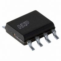
TJA1051T,118 NXP Semiconductors, TJA1051T,118 Datasheet - Page 9

TJA1051T,118
Manufacturer Part Number
TJA1051T,118
Description
IC CAN TXRX HI-SPEED 8-SOIC
Manufacturer
NXP Semiconductors
Type
Transceiverr
Datasheet
1.TJA1051T118.pdf
(21 pages)
Specifications of TJA1051T,118
Package / Case
8-SOIC (3.9mm Width)
Number Of Drivers/receivers
1/1
Protocol
CAN
Voltage - Supply
4.5 V ~ 5.5 V
Mounting Type
Surface Mount
Product
Controller Area Network (CAN)
Number Of Transceivers
1
Data Rate
1 Mbps
Supply Voltage (max)
5.5 V
Supply Voltage (min)
2.8 V or 4.5 V
Supply Current (max)
0.5 mA or 70 mA
Maximum Operating Temperature
+ 125 C
Minimum Operating Temperature
- 40 C
Mounting Style
SMD/SMT
Lead Free Status / RoHS Status
Lead free / RoHS Compliant
Lead Free Status / RoHS Status
Lead free / RoHS Compliant, Lead free / RoHS Compliant
Other names
935285281118
NXP Semiconductors
Table 7.
T
defined with respect to ground; Positive currents flow into the IC
[1]
[2]
[3]
[4]
[5]
[6]
11. Dynamic characteristics
Table 8.
T
defined with respect to ground. Positive currents flow into the IC.
TJA1051
Product data sheet
Symbol
V
V
V
V
I
I
I
R
ΔR
R
C
C
Temperature protection
T
Symbol
Transceiver timing; pins CANH, CANL, TXD and RXD; see
t
t
O(dom)
O(rec)
L
d(TXD-busdom)
d(TXD-busrec)
vj
vj
j(sd)
O(dif)bus
O(rec)
th(RX)dif
hys(RX)dif
i
i(dif)
i(cm)
i(dif)
=
=
i
Only TJA1051T/3 and TJA1051TK/3 have a V
All parameters are guaranteed over the virtual junction temperature range by design. Factory testing uses correlated test conditions to
cover the specified temperature and power supply voltage range.
Only TJA1051T/E has an EN pin.
Maximum value assumes V
Not tested in production; guaranteed by design.
V
−
−
cm(CAN)
40
40
°
°
C to +150
C to +150
Static characteristics
Dynamic characteristics
is the common mode voltage of CANH and CANL.
Parameter
bus differential output voltage V
recessive output voltage
differential receiver threshold
voltage
differential receiver hysteresis
voltage
dominant output current
recessive output current
leakage current
input resistance
input resistance deviation
differential input resistance
common-mode input
capacitance
differential input capacitance
shutdown junction
temperature
Parameter
delay time from TXD to bus dominant
delay time from TXD to bus recessive
°
°
C; V
C; V
CC
CC
CC
= 4.5 V to 5.5 V; V
= 4.5 V to 5.5 V; V
< V
IO
…continued
; if V
CC
All information provided in this document is subject to legal disclaimers.
> V
Conditions
V
R
V
Normal and Silent modes;
V
Normal and Silent modes
V
Normal and Silent modes
V
V
Normal and Silent modes; V
V
V
V
between V
IO
IO
TXD
CC
TXD
TXD
cm(CAN)
cm(CAN)
TXD
CANH
CC
CANH
L
pin CANH; V
pin CANL; V
pin. In transceivers without a V
IO
IO
, the maximum value will be V
= 45 Ω to 65 Ω
= 4.75 V to 5.25 V
= V
= 2.8 V to 5.5 V
= 2.8 V to 5.5 V
= 0 V; t < t
= V
= V
= 0 V; t < t
Rev. 6 — 25 March 2011
= V
= V
IO
[6]
IO
IO
= −30 V to +30 V
CANL
CANL
= 0 V;
CANH
Conditions
Normal mode
; recessive; no load
; no load
Normal mode
= −30 V to +30 V
CANL
CANH
= −27 V to +32 V
= 5 V
to(dom)TXD
to(dom)TXD
and V
Figure 3
[2]
[2]
= 5 V / 40 V
= 0 V
.
[1]
[1]
CANL
; R
; R
; V
L
L
= 60
= 60
and
CC
TXD
CC
IO
= 5 V
= V
Figure 4
pin, the V
Ω
Ω
+ 0.3 V.
unless specified otherwise; All voltages are
unless specified otherwise. All voltages are
IO
[5]
[5]
[5]
IO
Min
-
-
Min
1.5
−50
2
0.5
50
−100
40
−5
−5
9
−1
19
-
-
-
input is internally connected to V
High-speed CAN transceiver
Typ
65
90
Typ
-
-
0.5V
0.7
120
−70
70
-
0
15
0
30
-
-
190
Max
-
-
TJA1051
CC
© NXP B.V. 2011. All rights reserved.
Max
3
+50
3
0.9
200
−40
100
+5
+5
28
+1
52
20
10
-
Unit
ns
ns
CC
9 of 21
Unit
V
mV
V
V
mV
mA
mA
mA
μA
kΩ
%
kΩ
pF
pF
°C
.


