EL1508CM Intersil, EL1508CM Datasheet
EL1508CM
Specifications of EL1508CM
Available stocks


Related parts for EL1508CM


EL1508CM Summary of contents
Page 1
... All other trademarks mentioned are the property of their respective owners. EL1508 FN7014.5 differential output drive into 100Ω EL1508 (24 LD QFN) TOP VIEW VS THERMAL PAD GND 7 13 Intersil (and design registered trademark of Intersil Americas Inc. Copyright Intersil Americas Inc. 2001-2005, 2007. All Rights Reserved GND ...
Page 2
... EL1508CSZ (See Note) EL1508CSZ EL1508CSZ-T7 (See Note) EL1508CSZ EL1508CSZ-T13 (See Note) EL1508CSZ EL1508CM EL1508CM EL1508CM-T13 EL1508CM EL1508CMZ (See Note) EL1508CMZ EL1508CMZ-T13 (See Note) EL1508CMZ EL1508CL 1508CL EL1508CL-T7 1508CL EL1508CL-T13 1508CL EL1508CLZ (See Note) 1508CLZ EL1508CLZ-T7 (See Note) 1508CLZ EL1508CLZ-T13 (See Note) 1508CLZ NOTE: Intersil Pb-free plus anneal products employ special Pb-free material sets ...
Page 3
Absolute Maximum Ratings ( Supply Voltage -0.3V to 28V ...
Page 4
Electrical Specifications V = ±12V PARAMETER DESCRIPTION OUTPUT CHARACTERISTICS V Loaded Output Swing OUT I Linear Output Current OL I Output Current OUT DYNAMIC PERFORMANCE Bandwidth HD2 2nd Harmonic Distortion HD3 3rd Harmonic Distortion MTPR ...
Page 5
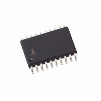
Pin Descriptions 16 Ld SOIC 20 Ld SOIC (0.150") (0.300" QFN ...
Page 6
Typical Performance Curves =2kΩ =±12V S R =100Ω =2.5kΩ R =0Ω F ADJ 20 R =3kΩ 100K 1M 10M FREQUENCY (Hz) FIGURE 1. DIFFERENTIAL FREQUENCY RESPONSE ...
Page 7
... V =±12V S R =3kΩ = =100Ω (kΩ) ADJ FIGURE 11. PEAKING EL1508 (Continued) 100pF 68pF 0pF 10M 100M FIGURE 8. EL1508CM SINGLE-ENDED CONFIGURATION L 150pF 100pF 62pF 39pF 22pF 5pF 10M 100M ADJ 26 V =±12V S R =3kΩ 150pF R =83Ω =0Ω SET 100pF 18 62pF ...
Page 8
Typical Performance Curves 10K 100K 1M FREQUENCY (Hz) FIGURE 13. OUTPUT IMPEDANCE 100 CURRENT NOISE 10 VOLTAGE NOISE 1 10 100 1K FREQUENCY (Hz) FIGURE 15. VOLTAGE AND CURRENT NOISE vs FREQUENCY 0.30 V =±12V ...
Page 9
Typical Performance Curves - 24 Ld QFN Package FREQ=1MHz -10 V =± SET R =100Ω L GAIN=10 -30 -50 -70 - (V) OUTP-P FIGURE 19. HARMONIC DISTORTION TEST (1/3 POWER ...
Page 10
Typical Performance Curves - 20 Ld SOIC (0.300") Package 0 FREQ=1MHz V =± SET -20 R =100Ω L GAIN=10 -40 HD2 -60 HD3 - (V) OUTP-P FIGURE 25. HARMONIC DISTORTION ...
Page 11
... POWER MODE) 0 FREQ=1MHz V =±12V S R =6.81kΩ SET -20 R =100Ω L GAIN=10 - -60 - (V) OUTP-P FIGURE 33. EL1508CM HARMONIC DISTORTION vs DIFFERENTIAL OUTPUT VOLTAGE (FULL POWER MODE) V OUT 40ns/DIV FIGURE 35. DISABLE TIME 11 EL1508 FIGURE 32. EL1508CL HARMONIC DISTORTION TEST FIGURE 34. EL1508CL HARMONIC DISTORTION TEST 2V/DIV FREQ=1MHz -10 V =± ...
Page 12
Typical Performance Curves 21.6 21.4 21.2 21.0 20.8 20 110 130 DIFFERENTIAL LOAD RESISTANCE (Ω) FIGURE 37. LOAD RESISTANCE vs OUTPUT VOLTAGE (ALL POWER MODES SUPPLY ...
Page 13
Applications Information The EL1508 consists of two high-power line driver amplifiers that can be connected for full duplex differential line transmission. The amplifiers are designed to be used with signals up to 4MHz and produce low distortion levels. The EL1508 ...
Page 14
quiescent output-stage × ( × ) × – OUT-RMS ...
Page 15
... TOP (16 Ld SO) INTERNAL GROUND PLANE (16 Ld SO) EL1508CM PCB Layout Considerations The 20 Ld SOIC (0.300") Power Package is designed so that heat may be conducted away from the device in an efficient manner. To disperse this heat, the center four leads on either side of the package are internally fused to the mounting platform of the die ...
Page 16
... Accordingly, the reader is cautioned to verify that data sheets are current before placing orders. Information furnished by Intersil is believed to be accurate and reliable. However, no responsibility is assumed by Intersil or its subsidiaries for its use; nor for any infringements of patents or other rights of third parties which may result from its use ...
Page 17
Small Outline Package Family (SO PIN #1 I.D. MARK 0.010 SEATING PLANE 0.004 C 0.010 MDP0027 SMALL OUTLINE PACKAGE FAMILY (SO) SYMBOL SO-8 SO-14 ...
Page 18
QFN (Quad Flat No-Lead) Package Family PIN #1 3 I.D. MARK 2X 0.075 C TOP VIEW 0. (E2) 7 (D2) BOTTOM VIEW 0. SEATING PLANE 0.08 C ...