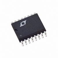
LTC1064-7CSW Linear Technology, LTC1064-7CSW Datasheet - Page 10

LTC1064-7CSW
Manufacturer Part Number
LTC1064-7CSW
Description
IC FILTR 8TH ORDR LOWPASS 16SOIC
Manufacturer
Linear Technology
Datasheet
1.LTC1064-7CN.pdf
(16 pages)
Specifications of LTC1064-7CSW
Filter Type
Linear Phase, Lowpass Switched Capacitor
Frequency - Cutoff Or Center
100kHz
Number Of Filters
1
Max-order
8th
Voltage - Supply
±2.375 V ~ 8 V
Mounting Type
Surface Mount
Package / Case
16-SOIC (0.300", 7.5mm Width)
Lead Free Status / RoHS Status
Contains lead / RoHS non-compliant
Other names
LTC1064-7CS
Available stocks
Company
Part Number
Manufacturer
Quantity
Price
Company:
Part Number:
LTC1064-7CSW
Manufacturer:
NEC
Quantity:
6
Part Number:
LTC1064-7CSW
Manufacturer:
LT/凌特
Quantity:
20 000
PI FU CTIO S
LTC1064-7
Power Supply Pins (4, 12)
The V
a 0.1µF capacitor to an adequate analog ground. The
filter’s power supplies should be isolated from other
digital or high voltage analog supplies. A low noise linear
supply is recommended. Using a switching power supply
will lower the signal-to-noise ratio of the filter. The supply
during power-up should have a slew rate less than 1V/µs.
When V
above ground, a signal diode should clamp V
latch-up. Figures 2 and 3 show typical connections for
dual and single supply operation.
Clock Input Pin (11)
Any TTL or CMOS clock source with a square-wave output
and 50% duty cycle (±10%) is an adequate clock source
for the device. The power supply for the clock source
should not be the filter’s power supply. The analog ground
10
V
V
V
V
IN
10k
10k
Figure 3. Single Supply Operation for an f
IN
+
+
U
Figure 2. Dual Supply Operation for an f
0.1µF
+
(Pin 4) and the V
+
0.1µF
is applied before V
U
1
2
3
4
5
6
7
+
LTC1064-7
1
2
3
4
5
6
7
1µF
U
LTC1064-7
–
(Pin 12) should be bypassed with
14
13
12
11
10
9
8
V
–
+
14
13
12
11
10
0.1µF
9
8
and V
200Ω
V
200Ω
+
CLK
–
CLK
is allowed to go
V
V
/f
/f
OUT
–
CUTOFF
DIGITAL SUPPLY
CLOCK SOURCE
GND
CUTOFF
DIGITAL SUPPLY
V
CLOCK SOURCE
GND
OUT
–
to prevent
= 50:1
= 50:1
1064-7 F02
1064-7 F03
+
+
for the filter should be connected to clock’s ground at a
single point only. Table 7 shows the clock’s low and high
level threshold values for a dual or single supply operation.
A pulse generator can be used as a clock source provided
the high level ON time is greater than 0.1µs. Sine waves are
not recommended for clock input frequencies less than
100kHz, since excessively slow clock rise or fall times
generate internal clock jitter (maximum clock rise or fall
time ≤ 1µs). The clock signal should be routed from the
right side of the IC package and perpendicular to it to avoid
coupling to any input or output analog signal path. A 200Ω
resistor between clock source and pin 11 will slow down
the rise and fall times of the clock to further reduce charge
coupling (Figures 2 and 3).
Analog Ground Pins (3, 5)
The filter performance depends on the quality of the
analog signal ground. For either dual or single supply
operation, an analog ground plane surrounding the pack-
age is recommended. The analog ground plane should be
connected to any digital ground at a single point. For dual
supply operation, Pin 3 should be connected to the analog
ground plane. For single supply operation pin 3 should be
biased at 1/2 supply and should be bypassed to the analog
ground plane with at least a 1µF capacitor (Figure 3). For
single 5V operation at the highest f
should be biased at 2V. This minimizes passband gain and
phase variations.
Ratio Input Pin (10)
The DC level at this pin determines the ratio of the clock
frequency to the cutoff frequency of the filter. Pin 10 at V
gives a 50:1 ratio and Pin 10 at V
single supply operation the ratio is 50:1 when Pin 10 is at
V
tied to ground, it should be bypassed to analog ground
Table 7. Clock Source High and Low Threshold Levels
POWER SUPPLY
Dual Supply = ±7.5V
Dual Supply = ±5V
Dual Supply = ± 2.5V
Single Supply = 12V
Single Suppl = 5V
+
and 100:1 when Pin 10 is at ground. When Pin 10 is not
HIGH LEVEL
≥ 2.18V
≥ 1.45V
≥ 0.73V
≥ 7.80V
≥ 1.45V
–
gives a 100:1 ratio. For
CLK
of 2MHz, Pin 3
LOW LEVEL
≤ – 2.0V
≤ 0.5V
≤ 0.5V
≤ 6.5V
≤ 0.5V
10647fb
+


