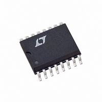
LTC1064-7CSW Linear Technology, LTC1064-7CSW Datasheet - Page 11

LTC1064-7CSW
Manufacturer Part Number
LTC1064-7CSW
Description
IC FILTR 8TH ORDR LOWPASS 16SOIC
Manufacturer
Linear Technology
Datasheet
1.LTC1064-7CN.pdf
(16 pages)
Specifications of LTC1064-7CSW
Filter Type
Linear Phase, Lowpass Switched Capacitor
Frequency - Cutoff Or Center
100kHz
Number Of Filters
1
Max-order
8th
Voltage - Supply
±2.375 V ~ 8 V
Mounting Type
Surface Mount
Package / Case
16-SOIC (0.300", 7.5mm Width)
Lead Free Status / RoHS Status
Contains lead / RoHS non-compliant
Other names
LTC1064-7CS
Available stocks
Company
Part Number
Manufacturer
Quantity
Price
Company:
Part Number:
LTC1064-7CSW
Manufacturer:
NEC
Quantity:
6
Part Number:
LTC1064-7CSW
Manufacturer:
LT/凌特
Quantity:
20 000
PI FU CTIO S
Clock Feedthrough
Clock feedthrough is defined as the RMS value of the clock
frequency and its harmonics that are present at the filter’s
output pin (9). The clock feedthrough is tested with the
input pin (2) grounded and it depends on PC board layout
and on the value of the power supplies. With proper layout
techniques the values of the clock feedthrough are shown
in Table 8.
Table 8. Clock Feedthrough
Note: The clock feedthrough at single 5V is imbedded in the
wideband noise of the filter. Clock waveform is a square wave.
A
Any parasitic switching transients during the rise and fall
edges of the incoming clock are not part of the clock
feedthrough specifications. Switching transients have fre-
quency contents much higher than the applied clock; their
with a 0.1µF capacitor. If the DC level at Pin 10 is switched
mechanically or electrically at slew rates greater than
1V/µs while the device is operating, a 10k resistor should
be connected between Pin 10 and the DC source.
Filter Input Pin (2)
The input pin is connected internally through a 40k resis-
tor tied to the inverting input of an op amp.
Filter Output Pins (9, 6)
Pin 9 is the specified output of the filter; it can typically
source 3mA and sink 1mA. Driving coaxial cables or
resistive loads less than 20k will degrade the total har-
monic distortion of the filter. When evaluating the device’s
distortion an output buffer is required. A noninverting
buffer, Figure 4, can be used provided that its input
common mode range is well within the filter’s output
swing. Pin 6 is an intermediate filter output providing an
unspecified 6th order lowpass filter. Pin 6 should not be
loaded.
PPLICATI
V
Single 5V
±5V
±7.5V
U
S
U
O
100µV
120µV
90µV
U
U
50:1
S
RMS
RMS
RMS
I FOR ATIO
U
W
100µV
300µV
650µV
100:1
RMS
RMS
RMS
U
External Connection Pins (7, 14)
Pins 7 and 14 should be connected together. In a printed
circuit board the connection should be done under the IC
package through a short trace surrounded by the analog
ground plane.
NC Pins (1, 5, 8, 13)
Pins 1, 5, 8 and 13 are not connected to any internal circuit
point on the device and should preferably be tied to analog
ground.
amplitude strongly depends on scope probing techniques
as well as grounding and power supply bypassing. The
clock feedthrough, if bothersome, can be greatly reduced
by adding a simple R/C lowpass network at the output of
the filter pin (9). This R/C will completely eliminate any
switching transients.
Wideband Noise
The wideband noise of the filter is the total RMS value of
the device’s noise spectral density and it is used to
determine the operating signal-to-noise ratio. Most of its
frequency contents lie within the filter passband and it
cannot be reduced with post filtering. For instance, the
LTC1064-7 wideband noise at ±5V supply is 105µV
95µV
the filter’s cutoff frequency. The total wideband noise
(µV
The clock feedthrough specifications are not part of the
wideband noise.
RMS
RMS
) is nearly independent of the value of the clock.
of which have frequency contents from DC up to
Figure 4. Buffer for Filter Output
1k
–
+
LT1220
1064-7 F04
LTC1064-7
11
10647fb
RMS
,


