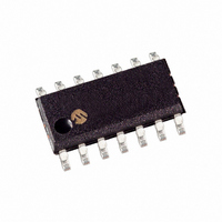
MCP25055-I/SL Microchip Technology, MCP25055-I/SL Datasheet - Page 41

MCP25055-I/SL
Manufacturer Part Number
MCP25055-I/SL
Description
IC I/O EXPANDER CAN 8B 14SOIC
Manufacturer
Microchip Technology
Specifications of MCP25055-I/SL
Package / Case
14-SOIC (3.9mm Width), 14-SOL
Interface
1-Wire, CAN
Number Of I /o
8
Interrupt Output
No
Frequency - Clock
4MHz
Voltage - Supply
2.7 V ~ 5.5 V
Operating Temperature
-40°C ~ 85°C
Mounting Type
Surface Mount
Includes
ADC, Memory, PWM
Product
Controller Area Network (CAN)
Number Of Transceivers
1
Data Rate
1 Mbps
Supply Voltage (max)
5.5 V
Supply Voltage (min)
2.7 V
Supply Current (max)
20 mA
Maximum Operating Temperature
+ 150 C
Minimum Operating Temperature
- 65 C
Mounting Style
SMD/SMT
Lead Free Status / RoHS Status
Lead free / RoHS Compliant
Other names
MCP25055I/SL
Available stocks
Company
Part Number
Manufacturer
Quantity
Price
Company:
Part Number:
MCP25055-I/SL
Manufacturer:
Microchip Technology
Quantity:
135
Company:
Part Number:
MCP25055-I/SL
Manufacturer:
Microchip Technology
Quantity:
184
7.0
7.1
The Analog-to-Digital (A/D) module is a four-channel,
10-bit successive approximation type of A/D. The A/D
allows conversion of an analog input signal to a
corresponding 10-bit number. The four channels are
multiplexed on the GP[3:0] pins. The converter is
turned off/on via the ADCON0 register and each
channel is individually enabled via the ADCON1 control
register. The V
selectable as internal or external. Each channel can be
set to one of two conversion modes:
1.
2.
7.2
The A/D module itself has several registers. The
registers are:
• A/D Control Register 0 (ADCON0)
• A/D Control Register 1 (ADCON1)
• Transmit-on-Change Register (IOINTEN)
• Compare and Polarity Register (ADCMPnL)
• A/D Result Registers (ADRESnL, ADRESnH)
The ADCON0 register controls the operation of the
A/D module, including auto-conversion rate and enable
bit. The ADCON1 register enables the A/D function on
port pins GP3:GP0, A/D conversion rate and selects
the voltage reference source. The IOINTEN register’s
four least significant bits enable/disable the transmit-
on-change function. The ADCMPnL.ADPOL bit sets
the polarity (above or below threshold) for the transmit-
on-change function.
The result of an A/D conversion is made available to
the user within the data field of the Read A/D Registers
output message via the CAN bus. This message can
be directly requested by another CAN node or be
automatically transmitted (TXIDO), as has been
described previously.
Additionally, the individual channel results may be read
using the “Read Register” command as described in
Section 4.3.1 “Information Request Messages” and
as shown in Table 3-2 by addressing the appropriate
A/D result register (ADRESnL and ADRESnH).
© 2007 Microchip Technology Inc.
Note:
Auto-conversion
Convert-on-request.
ANALOG-TO-DIGITAL
CONVERTER (A/D) MODULE
Description
A/D Module Registers
The GPDDR register controls the direction
of the GPIO pins, even when they are
being used as analog inputs. The user
must ensure that the bits in the GPDDR
register are maintained set (input) when
using them as analog inputs.
REF
+ and V
REF
- sources are user-
7.3
There are two modes of conversion that can be
individually selected for each analog channel that has
been enabled. These are auto-conversion and
conversion-on-request.
7.3.1
If the Auto-conversion mode is selected (STCON), an
A/D conversion is performed sequentially for each
channel that has been set to Analog Input mode and
has been configured for Auto-conversion mode.
Conversion starts with AN0 and is immediately
followed by AN1, etc. Once the conversion has
completed, the value is stored in the analog channel
registers for the respective channel.
The rate of the auto-conversion is determined by a
timer and prescaler. The formula for determining
conversion rates is:
Typical conversion rates with a 20 MHz oscillator input
are shown in Table 7-1.
TABLE 7-1:
The timer is turned on if one of the GPnTXC bits are set
in the IOINTEN register and configured as analog
input.
The prescaler counter is cleared when the device is
reset (RST reset or Power-on reset).
TOPS[2:0]
000
001
010
011
100
101
110
111
A/D Conversion Modes
AUTO-CONVERSION MODE
(
T
OSC
MCP2502X/5X
AUTO-CONVERSION RATES
FOR GIVEN PRESCALE
RATES AT 20 MHZ
) 1024
Prescale
(
1:1024
1:2048
1:4096
1:128
1:512
Rate
1:32
1:1
1:8
) Prescaler rate
(
Auto-Conversion
DS21664D-page 41
105 ms
210 ms
410 µs
)
26 ms
52 ms
51 µs
Rate
2 ms
7 ms


