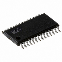
PCA9575PW2,118 NXP Semiconductors, PCA9575PW2,118 Datasheet - Page 2

PCA9575PW2,118
Manufacturer Part Number
PCA9575PW2,118
Description
IC I2C/SMBUS 16BIT GPIO 28-TSSOP
Manufacturer
NXP Semiconductors
Series
-r
Datasheet
1.PCA9575HF118.pdf
(38 pages)
Specifications of PCA9575PW2,118
Interface
I²C, SMBus
Number Of I /o
16
Interrupt Output
Yes
Frequency - Clock
400kHz
Voltage - Supply
1.1 V ~ 3.6 V
Operating Temperature
-40°C ~ 85°C
Mounting Type
Surface Mount
Package / Case
28-TSSOP
Includes
POR
Description/function
16-bit I2C-bus and SMBus
Maximum Operating Temperature
+ 85 C
Minimum Operating Temperature
- 40 C
Mounting Style
SMD/SMT
Supply Voltage (max)
3.6 V
Supply Voltage (min)
1.1 V
Lead Free Status / RoHS Status
Lead free / RoHS Compliant
Other names
935286414118
NXP Semiconductors
2. Features
PCA9575_3
Product data sheet
Power-On Reset (POR) or hardware reset pin (RESET) initializes the two banks of 8 I/Os
as inputs, sets the registers to their default values and initializes the device state machine.
The I/O banks are held in its default state when the logic supply (V
The PCA9575 is available in 24-pin TSSOP, 28-pin TSSOP and HWQFN24 packages,
and is specified over the 40 C to +85 C industrial temperature range.
The 28-pin package provides four address select pins, allowing up to 16 PCA9575
devices to be connected with 16 different addresses on the same I
I
I
I
I
I
I
I
I
I
I
I
I
I
I
I
Separate supply rails for core logic and each of the two I/O banks provides voltage
level shifting
1.1 V to 3.6 V operation with level shifting feature
Very low standby current: < 2 A
16 configurable I/O pins organized as 2 banks that default to inputs at power-up
Outputs:
Inputs:
400 kHz I
Compliant with I
Active LOW reset (RESET) input pin resets device to power-up default state
GPIO All Call address allows programming of more than one device at the same time
with the same parameters
16 programmable slave addresses using 4 address pins (28-pin TSSOP only)
ESD protection exceeds 6000 V HBM per JESD22-A114, 500 V MM per
JESD22-A115, and 1000 V CDM per JESD22-C101
Latch-up testing is done to JEDEC Standard JESD78 which exceeds 100 mA
Packages offered: TSSOP28, TSSOP24, HWQFN24
N
N
N
N
N
N
40 C to +85 C operation
Totem pole: 1 mA source and 3 mA sink
Independently programmable 100 k pull-up or pull-down for each I/O pin
Open-drain active LOW interrupt (INT) output pin allows monitoring of logic level
change of pins programmed as inputs
Programmable bus hold provides valid logic level when inputs are not actively
driven
Programmable Interrupt Mask Control for input pins that do not require an interrupt
when their states change or to prevent spurious interrupts default to mask at
power-up
Polarity Inversion register allows inversion of the polarity of the I/O pins when read
2
C-bus serial interface
2
C-bus Standard-mode (100 kHz)
Rev. 03 — 9 November 2009
16-bit I
2
C-bus and SMBus, level translating, low voltage GPIO
DD
2
C-bus.
) is off.
PCA9575
© NXP B.V. 2009. All rights reserved.
2 of 38


