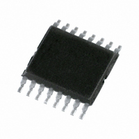
PCA9556PW,112 NXP Semiconductors, PCA9556PW,112 Datasheet - Page 4

PCA9556PW,112
Manufacturer Part Number
PCA9556PW,112
Description
IC I/O EXPANDER I2C 8B 16TSSOP
Manufacturer
NXP Semiconductors
Datasheet
1.PCA9556PW118.pdf
(13 pages)
Specifications of PCA9556PW,112
Package / Case
16-TSSOP
Interface
I²C, SMBus
Number Of I /o
8
Interrupt Output
Yes
Frequency - Clock
100KHz
Voltage - Supply
3 V ~ 5.5 V
Operating Temperature
-40°C ~ 85°C
Mounting Type
Surface Mount
Includes
POR
Logic Family
PCA9556
Number Of Lines (input / Output)
8.0 / 8.0
Operating Supply Voltage
3 V to 5.5 V
Operating Temperature Range
- 40 C to + 85 C
Logic Type
I2C, SMBus
Mounting Style
SMD/SMT
Number Of Input Lines
8.0
Number Of Output Lines
8.0
Output Current
20 mA
Lead Free Status / RoHS Status
Lead free / RoHS Compliant
Lead Free Status / RoHS Status
Lead free / RoHS Compliant, Lead free / RoHS Compliant
Other names
568-1059-5
935262899112
PCA9556PW
935262899112
PCA9556PW
a write transmission. It is used as a pointer to determine which of the
of the pins, regardless of whether the pin is defined as an input or an
Philips Semiconductors
REGISTERS
Command Byte
The command byte is the first byte to follow the address byte during
following registers will be written or read.
Register 0 — Input Port Register
This register is an read-only port. It reflects the incoming logic levels
output by register 3. Writes to this register have no effect.
Register 1 — Output Port Register
This register reflects the outgoing logic levels of the pins defined as
outputs by register 3. Bit values in this register have no effect on
pins defined as inputs. In turn, reads from this register reflect the
value that is in the flip-flop controlling the output selection, NOT the
actual pin value.
2002 Mar 28
default
Command
Octal SMBus and I
bit
I7
0
1
2
3
O7
I6
0
Read/write byte
Read/write byte
Read/write byte
O6
0
Read byte
I5
Protocol
O5
0
I4
O4
0
2
C registered interface
I3
Function
Polarity inversion register
Configuration register
Input port register
Output port register
O3
0
I2
O2
0
I1
O1
0
I0
O0
0
4
Register 2 — Polarity Inversion Register
This register enables polarity inversion of pins defined as inputs by
register 3. If a bit in this register is set (written with ‘1’), the
corresponding port pin’s polarity is inverted. If a bit in this register is
cleared (written with a ‘0’), the corresponding port pin’s original
polarity is retained.
Register 3 — Configuration Register
This register configures the directions of the I/O pins. If a bit in this
register is set, the corresponding port pin is enabled as an input with
high impedance output driver. If a bit in this register is cleared, the
corresponding port pin is enabled as an output.
RESET
Power-on Reset
When power is applied to V
PCA9556 in a reset state until V
the reset condition is released and the PCA9556 registers and
SMBus state machine will initialize to their default states.
External Reset
A reset can be accomplished by holding the RESET pin low for a
minimum of T
machine will be held in their default state until the RESET input is
once again high. This input typically requires a pull-up to 3.3 V V
default
default
bit
bit
C7
N7
1
1
W
. The PCA9556 registers and SMBus/I
C6
N6
1
1
C5
N5
1
1
DD
, an internal power-on reset holds the
DD
C4
N4
1
1
has reached V
C3
N3
1
0
C2
N2
PCA9556
1
0
POR
2
. At that point,
C state
C1
Product data
N1
0
1
N0
C0
1
0
CC.


