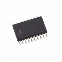
HIP9011AB Intersil, HIP9011AB Datasheet - Page 8

HIP9011AB
Manufacturer Part Number
HIP9011AB
Description
IC SENSOR ENGINE KNOCK 20-SOIC
Manufacturer
Intersil
Type
Engine Knock Signal Processorr
Datasheet
1.HIP9011ABZ.pdf
(11 pages)
Specifications of HIP9011AB
Input Type
Logic
Output Type
Logic
Interface
SPI
Current - Supply
8mA
Mounting Type
Surface Mount
Package / Case
20-SOIC (7.5mm Width)
Lead Free Status / RoHS Status
Contains lead / RoHS non-compliant
Available stocks
Company
Part Number
Manufacturer
Quantity
Price
Company:
Part Number:
HIP9011AB
Manufacturer:
INTERSIL
Quantity:
20 478
Company:
Part Number:
HIP9011AB
Manufacturer:
INTERSIL
Quantity:
19 565
Part Number:
HIP9011AB
Manufacturer:
INTERSIL
Quantity:
20 000
Company:
Part Number:
HIP9011ABR4818
Manufacturer:
INTERSIL
Quantity:
7 306
Company:
Part Number:
HIP9011ABR7007
Manufacturer:
INTERSIL
Quantity:
6 665
Part Number:
HIP9011ABT
Manufacturer:
INTERSIL
Quantity:
20 000
Company:
Part Number:
HIP9011ABTS2457
Manufacturer:
PH
Quantity:
7 320
Part Number:
HIP9011ABZ
Manufacturer:
HAR
Quantity:
20 000
Part Number:
HIP9011ABZT
Manufacturer:
INTERSIL
Quantity:
20 000
Integration is enabled by the rising edge of the input control
signal INT/HOLD. Within 20µs after the integrate input
reaches a logic high level, the output of the integrator will fall
to approximately V
integrator is an analog voltage.
Differential to Single-Ended Converter
This circuit takes the differential output of the integrators
(through the test-multiplexer circuit) and provides a signal
that is the sum of the two signals. This technique is used to
improve the noise immunity of the system.
Output Buffer
This output amplifier is the same amplifier circuits as the
input amplifier used to interface with the sensors. For
diagnostic purposes when the output of the antialias filter is
being evaluated, this amplifier is in the power down mode.
Test Multiplexer
This circuit receives the positive and negative outputs from
the integrator, together with the outputs from different parts
of the IC. The Test Mux output is controlled by the fifth
programming word of the communications protocol. This
multiplexes the switch capacitor filter output, the gain control
output and the antialias filter output.
SPI Communications Protocol
Communicating to the Knock Sensor via the SPI Bus
(MOSI). A chip select pin (CS) is used to enable the chip,
which, in conjunction with the SPI clock (SCK), which moves
an eight bit programming word. Five different programming
words are used to set the following internal programmable
registers: GAIN, BANDPASS FREQUENCY FILTER,
INTEGRATOR TIME CONSTANT, CHANNEL SELECT, SO
output mode, and TEST MODES.
When chip select (CS) goes low, on the next falling edge of
the SPI clock (SCK), data is latched into the SPI register.
The data is shifted with the most significant bit first and least
significant bit last. Each word is divided into two parts: first
the address and then the value. Depending on the function
being controlled, the address is 2 or 3 bits, and the value is
either 5 or 6 bits long. All five programming words can be
entered into the IC during the HOLD mode of operation. The
integration or hold mode of operation is controlled by the
INT/HOLD input signal.
RESET
, 0.125V. The output of the
8
HIP9011
Programming Words
1. Band Pass Filter Frequency: Defines the center
2. Gain Control: defines the value of the gain stage
3. Integrator Time Constant: Defines the Integration Time
4. Test/Channel Select Control: Again the first three bits, 111
5. Prescaler/SO terminal status: Defines the division ratio of
A) If B0 is “0”, than channel 0 is selected. If B0 is “1”;
B) The remaining bits are used for selection of the various
frequency of the Band Pass Filter in the system. The first
2 bits are used for the address and the last 6 bits are used
for its value. 00FFFFFF Example: 00001010 would be
the Band Pass Filter at a center frequency of 1.78kHz (bit
value of 10 in Table 3).
attenuation of gain setting. The first 2 bits are again used
for the address and the last 6 bits for its value.
10GGGGGG Example: 10010100 would be the Gain
Control (10 for the first two bits) with an attenuation of
0.739 (bit value of 20 in Table 3).
Constant for the system. The first 3 bits are used for the
address and the last 5 bits for the value. 110TTTTT
Example: 11000011 would be the Integrator Time
Constant (110 for the first 3 bits) and an Integration Time
Constant of 55µs (bit value 3 in Table 3).
are the address for this function, and the last five bits
define the functions that may be programmed. Example:
111B4B3B2B1B0; The options are:
the internal frequency prescaler and the status of the SO
terminal, pin 11. P1 to P4 bits define the frequency that
may be used with an external clock. The status of the
three state SO pin is set by the last, Z bit.
01P5P4P3P2P1Z; Example: 0100000, Note, in this case
bit P5 is not used. (01 for the first 2 bits sets the
Prescaler/SO function) P1 to P4 set Prescaler for a clock
frequency of 4MHz and the last bit sets the S0 terminal to
an active state.
than channel 1 is selected as the input.
diagnostic modes. TEST pin (14) = low. Not applicable
in Run Mode.
January 6, 2006
FN4367.2


