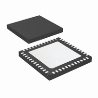
DS32ELX0421SQX/NOPB National Semiconductor, DS32ELX0421SQX/NOPB Datasheet - Page 18

DS32ELX0421SQX/NOPB
Manufacturer Part Number
DS32ELX0421SQX/NOPB
Description
IC SERIALIZER 312.5GBPS 48LLP
Manufacturer
National Semiconductor
Datasheet
1.DS32EL0421SQENOPB.pdf
(28 pages)
Specifications of DS32ELX0421SQX/NOPB
Function
Serializer
Data Rate
3.125Gbps
Input Type
LVDS
Output Type
CML
Number Of Inputs
5
Number Of Outputs
2
Voltage - Supply
2.5V, 3.3V
Operating Temperature
-40°C ~ 85°C
Mounting Type
Surface Mount
Package / Case
48-LLP
Lead Free Status / RoHS Status
Lead free / RoHS Compliant
Other names
DS32ELX0421SQX
www.national.com
Applications Information
GPIO PINS
The GPIO pins can be useful tools when debugging or eval-
uating the system. For specific GPIO configurations and func-
tions refer to registers 2, 3, 4, 5 and 6 in the device register
map.
GPIO pins are commonly used when there are multiple seri-
alizers on the same SMBus. In order to program individual
settings into each serializer, they will each need to have a
unique SMBus address. To reprogram multiple serializers on
a single SMBus, configure the first serializer such that the
SMBus lines are connected to the FPGA or host controller.
The CS pin of the second serializer should be tied to GPIO0
of the first serializer, with the CS pin of the next serializer tied
to GPIO0 of its preceding serializer. By holding all of the
GPIO0 pins low, the first serializer’s address may now be re-
programmed by writing to register 0. The first serializer’s
GPIO pin can now be asserted and the second serializer’s
address may now be reprogrammed.
HIGH SPEED COMMUNICATION MEDIA
Using the serializer’s integrated de-emphasis blocks in com-
bination with the DS32EL0124 or DS32ELX0124’s integrated
equalization blocks allows data to be transmitted across a
variety of media at high speeds. Factors that can limit device
performance include excessive input clock jitter, noisy power
rails, EMI from nearby noisy components and poor layout
techniques. Although many cables contain wires of similar
gauge and shielding, performance can vary greatly depend-
ing on the quality of the connector.
REDUNDANCY APPLICATIONS
The DS32ELX0421 has two high speed CML serial outputs.
SMBus register control allows the device to use a single out-
put exclusively, or both outputs simultaneously. This allows a
single serializer to transmit data to two independant receiving
systems, a primary and secondary endpoint. Some applica-
tions require a redundancy measure in case the primary
signal path is compromised. The secondary output can be
activated “on-the-go”, if a problem is detected on the primary
18
link. See the
located under
LINK AGGREGATION
Multiple
D32EL0124/DS32ELX0124 deserializers can be aggregated
together if an application requires a data throughput of more
than 3.125 Gbps. By utilizing the data valid signal of each
device, the system can be properly deskewed to allow for a
single cable, such as CAT-6, DVI-D, or HDMI, to carry data
payloads beyond 3.125 Gbps.
Link aggregation configurations can also be implemented in
applications which require longer cable lengths. In these type
of applications the data rate of each serializer and deserializer
chipset can be reduced, such that the applications' net data
throughput is still the same. Since each high speed channel
is now operating at a fraction of the original data rate, the loss
over the cable is reduced, allowing for greater lengths of cable
to be used in the system.
For more information regarding link aggregation please see
Application Note 1887, Expanding the Payload with National's
FPGA-Link DS32ELX0421 and DS32ELX0124 Serializer and
Deserializer.
LAYOUT GUIDELINES
It is important to follow good layout practices for high speed
devices. The length of LVDS input traces should not exceed
40 inches. In noisy environment the LVDS traces may need
to be shorter to prevent data corruption due to EMI. Noisy
components should not be placed next to the LVDS or CML
traces. The LVDS and CML traces must have a controlled
differential impedance of 100 Ω. Do not place termination re-
sistor at the LVDS inputs or CML outputs, the DS32EL0421
and DS32ELX0421 have internal termination resistors. It is
recommended to avoid using vias. Vias create an impedance
mismatch in the transmission line and result in reflections,
which can greatly lower the maximum distance of the high
speed data link. If vias are required, they should be placed
symmetrically on each side of the differential pair. For more
tips and detailed suggestions regarding high speed board
layout principles, please consult the LVDS Owner’s Manual.
DS32EL0421/DS32ELX0421
Redundancy / Fail Over Configuration
Register
Recipes.
serializers
section
and


