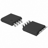
PCA9515DP,118 NXP Semiconductors, PCA9515DP,118 Datasheet - Page 7

PCA9515DP,118
Manufacturer Part Number
PCA9515DP,118
Description
IC I2C BUS REPEATER 8-TSSOP
Manufacturer
NXP Semiconductors
Type
Repeaterr
Datasheet
1.PCA9515DP118.pdf
(16 pages)
Specifications of PCA9515DP,118
Package / Case
8-TSSOP
Tx/rx Type
I²C Logic
Delay Time
55ns
Capacitance - Input
6pF
Voltage - Supply
3 V ~ 3.6 V
Current - Supply
2.3mA
Mounting Type
Surface Mount
Logic Family
PCA9515
Operating Supply Voltage
2.3 V to 3.6 V
Power Dissipation
100 mW
Operating Temperature Range
- 40 C to + 85 C
Input Voltage
5.5 V
Logic Type
I2C Bus
Maximum Clock Frequency
400 KHz
Mounting Style
SMD/SMT
Output Current
50 mA
Output Voltage
5.5 V
Lead Free Status / RoHS Status
Lead free / RoHS Compliant
For Use With
OM6285 - EVAL BOARD I2C-2002-1A568-4002 - DEMO BOARD I2C
Lead Free Status / Rohs Status
Lead free / RoHS Compliant
Other names
568-1034-2
935268635118
PCA9515DP-T
935268635118
PCA9515DP-T
NXP Semiconductors
9. Static characteristics
Table 5.
V
[1]
[2]
PCA9515_9
Product data sheet
Symbol
Supplies
V
I
I
I
Input SCLn; input/output SDAn
V
V
V
V
I
I
V
V
I
C
Enable input EN
V
V
I
I
C
CCH
CCL
CCLc
LI
IL
LOH
IL
LI
CC
CC
IH
IL
ILc
IK
OL
OL
IL
IH
i
i
= 3.0 V to 3.6 V; GND = 0 V; T
V
SDAn/SCLn lines.
The SCLn/SDAn C
repeater but an active bus remains on either set of SCLn/SDAn pins.
V
IL
ILc
specification is for the first LOW level seen by the SDAn/SCLn lines. V
Static characteristics
Parameter
supply voltage
HIGH-level supply current
LOW-level supply current
contention LOW-level supply current
HIGH-level input voltage
LOW-level input voltage
contention LOW-level input voltage
input clamping voltage
input leakage current
LOW-level input current
LOW-level output voltage
difference between LOW-level
output and LOW-level input voltage
contention
HIGH-level output leakage current
input capacitance
LOW-level input voltage
HIGH-level input voltage
LOW-level input current
input leakage current
input capacitance
i
is about 200 pF when V
amb
= 40 C to +85 C; unless otherwise specified.
CC
= 0 V. The PCA9515A should be used in applications where power is secured to the
Rev. 09 — 23 April 2009
Conditions
both channels HIGH;
V
SDAn = SCLn = V
both channels LOW;
V
and one SCL = GND,
other SDA and SCL open
V
SDAn = SCLn = GND
I
V
SDA, SCL; V
I
guaranteed by design
V
V
EN; V
V
I
OL
CC
CC
CC
I
O
I
I
= 18 mA
= 3.6 V
= 3 V or 0 V
= 3.0 V or 0 V
= 0 mA or 6 mA
= 3.6 V
= 3.6 V;
= 3.6 V; one SDA
= 3.6 V;
I
= 0.2 V
I
= 0.2 V
ILc
CC
is for the second and subsequent LOW levels seen by the
[1]
[1]
Min
3.0
-
-
-
0.7V
-
-
0.47
-
-
-
2.0
-
-
0.5
0.5
1
0.5
1
CC
Typ
3.3
2.3
2.3
2.1
-
-
-
-
-
-
0.52
-
-
6
-
-
10
-
6
PCA9515
© NXP B.V. 2009. All rights reserved.
I
2
Max
3.6
5
5
5
5.5
+0.3V
+0.4
+1
10
0.6
70
10
7
+0.8
5.5
30
+1
7
C-bus repeater
1.2
[2]
CC
Unit
V
mA
mA
mA
V
V
V
V
V
mV
pF
V
V
pF
7 of 16
A
A
A
A
A


