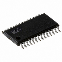
PCA9558PW,112 NXP Semiconductors, PCA9558PW,112 Datasheet - Page 7

PCA9558PW,112
Manufacturer Part Number
PCA9558PW,112
Description
IC I2C/SMBUS 8BIT 28-TSSOP
Manufacturer
NXP Semiconductors
Datasheet
1.PCA9558PW112.pdf
(27 pages)
Specifications of PCA9558PW,112
Applications
PC's, PDA's
Interface
I²C
Voltage - Supply
3 V ~ 3.6 V
Package / Case
28-TSSOP
Mounting Type
Surface Mount
Lead Free Status / RoHS Status
Lead free / RoHS Compliant
Other names
568-3399-5
935269433112
PCA9558PW
935269433112
PCA9558PW
NXP Semiconductors
PCA9558_4
Product data sheet
The Multiplexer function controls the six open-drain outputs, MUX_OUTx and
NON_MUXED_OUT. This control is affected by the input pins MUX_SELECT (pin 19),
MUX_OUT_LOW (pin 26), and/or an internal register programmed via the I
Upon power-up, the multiplex function is controlled by the MUX_SELECT and
MUX_OUT_LOW pins. When the MUX_SELECT signal is a logic 0, the multiplexer will
select the data from the 6-bit EEPROM to drive on the MUX_OUTx and
NON_MUXED_OUT pins. When the MUX_SELECT signal is a logic 1, the multiplexer will
select the MUX_INx pins to drive on the MUX_OUTx pins.
The NON_MUXED_OUT output is latched from the 6-bit EEPROM on a rising edge of the
MUX_SELECT signal. This latch is transparent while the MUX_SELECT signal is a
logic 0. An internal control register, written via the I
function. When this register is written, the MUX_SELECT function can change from the
external pin to an internal register. In this register a bit will act in a similar fashion to the
MUX_SELECT input, i.e., a logic 1 will cause the multiplexer to select data from the 6-bit
EEPROM to drive on the MUX_OUTx and NON_MUXED_OUT pins. In this configuration,
the NON_MUXED_OUT will latch data when the PCA9558 acknowledges the I
The MUX_SELECT pin will have no effect on the MUX_OUTx or NON_MUXED_OUT
while in this mode.
When the MUX_OUT_LOW signal is a logic 0 and the multiplexer is configured so that the
MUX_OUTx pins are being driven by the 6-bit EEPROM, the MUX_OUTx pins will be
driven to a logic 0. This information is summarized in
Table 4.
[1]
[2]
[3]
If the MUX_OUTx outputs are being driven by the 6-bit EEPROM and this EEPROM is
programmed, the outputs will remain stable and change to the new values after the
EEPROM program cycle completes.
Examples of read/write for MUX control can be found in
Register
B1
x
x
x
x
0
1
0
1
[1]
These are the 2 LSBs of the MUX Control (MUXCNTRL) register.
NON_MUXED_OUT value will be the value present in the 6-bit EEPROM at the time of the rising edge of
the MUX_SELECT input.
NON_MUXED_OUT value will be the value present in the 6-bit EEPROM at the time of the slave ACK when
bit 1 has changed from logic 0 to logic 1.
B0
0
0
0
0
1
1
1
1
[1]
Multiplexer function table
Input
MUX_OUT_LOW MUX_SELECT
0
0
1
1
0
0
1
1
Rev. 04 — 14 April 2009
1
0
1
0
x
x
x
x
Output
MUX_OUTx
MUX_INx inputs
0
MUX_INx inputs
from EEPROM
MUX_INx inputs
0
MUX_INx inputs
from EEPROM
2
C-bus, can also control the multiplexer
Table
Figure
8-bit I
4.
7.
2
NON_MUXED_OUT
latched from EEPROM
0
latched from EEPROM
from EEPROM
latched from EEPROM
0
latched from EEPROM
from EEPROM
C-bus/SMBus I/O port
PCA9558
© NXP B.V. 2009. All rights reserved.
2
C-bus.
2
C-bus.
7 of 27
[2]
[2]
[3]
[3]


