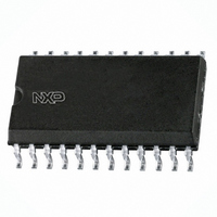
PCA9547D,118 NXP Semiconductors, PCA9547D,118 Datasheet - Page 5

PCA9547D,118
Manufacturer Part Number
PCA9547D,118
Description
IC MUX 8CH I2C BUS 24SOIC
Manufacturer
NXP Semiconductors
Datasheet
1.PCA9547BS118.pdf
(26 pages)
Specifications of PCA9547D,118
Package / Case
24-SOIC (7.5mm Width)
Applications
Translating Multiplexer
Interface
I²C, SMBus
Voltage - Supply
2.3 V ~ 3.6 V, 4.5 V ~ 5.5 V
Mounting Type
Surface Mount
Product
Decoders, Encoders, Multiplexers & Demultiplexers
Number Of Lines (input / Output)
8.0 / 1.0
Propagation Delay Time
0.3 ns at 2.3 V to 5.5 V
Supply Voltage (max)
5.5 V
Supply Voltage (min)
2.3 V
Maximum Operating Temperature
+ 85 C
Minimum Operating Temperature
- 40 C
Mounting Style
SMD/SMT
Number Of Input Lines
8.0
Number Of Output Lines
1.0
Lead Free Status / RoHS Status
Lead free / RoHS Compliant
Lead Free Status / RoHS Status
Lead free / RoHS Compliant, Lead free / RoHS Compliant
Other names
935280788118
PCA9547D-T
PCA9547D-T
PCA9547D-T
PCA9547D-T
NXP Semiconductors
PCA9547_3
Product data sheet
5.2 Pin description
Table 3.
[1]
Symbol
A0
A1
RESET
SD0
SC0
SD1
SC1
SD2
SC2
SD3
SC3
V
SD4
SC4
SD5
SC5
SD6
SC6
SD7
SC7
A2
SCL
SDA
V
SS
DD
HVQFN24 package die supply ground is connected to both the V
V
and board-level performance, the exposed pad needs to be soldered to the board using a corresponding
thermal pad on the board, and for proper heat conduction through the board thermal vias need to be
incorporated in the PCB in the thermal pad region.
SS
pin must be connected to supply ground for proper device operation. For enhanced thermal, electrical,
Pin description
Pin
SO24, TSSOP24
1
2
3
4
5
6
7
8
9
10
11
12
13
14
15
16
17
18
19
20
21
22
23
24
Rev. 03 — 10 July 2009
HVQFN24
22
23
24
1
2
3
4
5
6
7
8
9
10
11
12
13
14
15
16
17
18
19
20
21
[1]
Description
address input 0
address input 1
active LOW reset input
serial data output 0
serial clock output 0
serial data output 1
serial clock output 1
serial data output 2
serial clock output 2
serial data output 3
serial clock output 3
supply ground
serial data output 4
serial clock output 4
serial data output 5
serial clock output 5
serial data output 6
serial clock output 6
serial data output 7
serial clock output 7
address input 2
serial clock line
serial data line
supply voltage
8-channel I
SS
2
pin and the exposed center pad. The
C-bus multiplexer with reset
PCA9547
© NXP B.V. 2009. All rights reserved.
5 of 26


