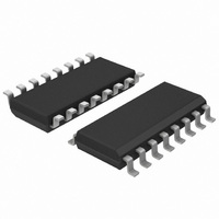
74HC4053D,652 NXP Semiconductors, 74HC4053D,652 Datasheet - Page 16

74HC4053D,652
Manufacturer Part Number
74HC4053D,652
Description
IC MUX/DEMUX TRIPLE 2X1 16SOIC
Manufacturer
NXP Semiconductors
Series
74HCr
Datasheet
1.74HC4053D653.pdf
(32 pages)
Specifications of 74HC4053D,652
Package / Case
16-SOIC (0.154", 3.90mm Width)
Function
Multiplexer/Demultiplexer
Circuit
3 x 2:1
On-state Resistance
60 Ohm
Voltage Supply Source
Dual Supply
Voltage - Supply, Single/dual (±)
±2 V ~ 10 V
Current - Supply
16µA
Operating Temperature
-40°C ~ 125°C
Mounting Type
Surface Mount
Propagation Delay Time
60 ns
Maximum Power Dissipation
500 mW
Maximum Operating Temperature
125 C
Minimum Operating Temperature
- 40 C
Mounting Style
SMD/SMT
Number Of Switches
Triple
Lead Free Status / RoHS Status
Lead free / RoHS Compliant
Lead Free Status / RoHS Status
Lead free / RoHS Compliant, Lead free / RoHS Compliant
Other names
568-3963-5
74HC4053D
74HC4053D
933714840652
74HC4053D
74HC4053D
933714840652
NXP Semiconductors
Table 9.
GND = 0 V; t
V
V
[1]
[2]
[3]
[4]
Table 10.
GND = 0 V; t
V
V
74HC_HCT4053
Product data sheet
Symbol
t
Symbol
T
t
t
off
pd
on
is
os
is
os
amb
is the input voltage at a nYn or nZ terminal, whichever is assigned as an input.
is the input voltage at a nYn or nZ terminal, whichever is assigned as an input.
is the output voltage at a nYn or nZ terminal, whichever is assigned as an output.
is the output voltage at a nYn or nZ terminal, whichever is assigned as an output.
t
t
t
C
P
f
f
N = number of inputs switching;
Σ{(C
C
C
V
pd
on
off
i
o
D
CC
PD
= input frequency in MHz;
L
sw
= 25 °C
= output frequency in MHz;
is the same as t
is the same as t
is the same as t
= output load capacitance in pF;
= C
= switch capacitance in pF;
L
is used to determine the dynamic power dissipation (P
= supply voltage in V.
+ C
PD
Parameter
propagation delay V
turn-on time
Parameter
turn-off time
Dynamic characteristics for 74HC4053
Dynamic characteristics for 74HCT4053
r
r
sw
× V
= t
= t
) × V
CC
f
f
= 6 ns; C
= 6 ns; C
2
CC
× f
PHL
PZH and
PHZ
2
i
× f
× N + Σ{(C
and t
and t
o
} = sum of outputs;
L
L
t
= 50 pF; for test circuit see
= 50 pF; for test circuit see
PZL
PLH
PLZ
.
Conditions
E to V
Sn to V
Conditions
E to V
Sn to V
.
.
L
is
V
V
V
V
V
V
V
V
V
V
V
V
V
V
V
V
+ C
to V
CC
CC
CC
CC
CC
CC
CC
CC
CC
CC
CC
CC
CC
CC
CC
CC
sw
os
os
= 4.5 V; V
= 4.5 V; V
= 4.5 V; V
= 5.0 V; V
= 4.5 V; V
= 4.5 V; V
= 5.0 V; V
= 4.5 V; V
= 2.0 V; V
= 4.5 V; V
= 6.0 V; V
= 4.5 V; V
= 2.0 V; V
= 4.5 V; V
= 6.0 V; V
= 4.5 V; V
os
os
os
) × V
; R
; R
; R
; R
; R
L
L
All information provided in this document is subject to legal disclaimers.
CC
L
L
L
= 1 kΩ; see
= 1 kΩ; see
= ∞ Ω; see
= 1 kΩ; see
= 1 kΩ; see
2
× f
EE
EE
EE
EE
EE
EE
EE
EE
EE
EE
EE
EE
EE
EE
EE
EE
o
} where:
Rev. 5 — 18 January 2011
= 0 V
= 0 V
= 0 V
= −4.5 V
= 0 V
= 0 V
= 0 V
= −4.5 V
= 0 V
= −4.5 V
= 0 V
= 0 V; C
= −4.5 V
= 0 V
= 0 V; C
= −4.5 V
…continued
Figure
Figure
Figure 14
Figure 14
Figure 13
D
Figure 14
Figure 14
in μW).
L
L
= 15 pF
= 15 pF
15.
15.
Triple 2-channel analog multiplexer/demultiplexer
74HC4053; 74HCT4053
[1]
[2]
[2]
[3]
[3]
Min
-
-
-
-
-
-
-
-
Min
-
-
-
-
-
-
-
-
Typ
-
-
-
-
-
-
-
-
Typ
5
4
27
23
16
25
21
16
© NXP B.V. 2011. All rights reserved.
Max
315
63
54
44
315
63
54
44
Max
12
8
48
-
34
48
-
34
Unit
ns
ns
ns
ns
ns
ns
ns
ns
Unit
ns
ns
ns
ns
ns
ns
ns
ns
16 of 32


