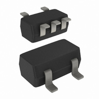
74LVC1G66GW,165 NXP Semiconductors, 74LVC1G66GW,165 Datasheet - Page 14

74LVC1G66GW,165
Manufacturer Part Number
74LVC1G66GW,165
Description
IC SWITCH SPST UMT5
Manufacturer
NXP Semiconductors
Series
74LVCr
Datasheet
1.74LVC1G66GM115.pdf
(25 pages)
Specifications of 74LVC1G66GW,165
Function
Switch
Circuit
1 x SPST- NO
On-state Resistance
6 Ohm
Voltage Supply Source
Single Supply
Voltage - Supply, Single/dual (±)
1.65 V ~ 5.5 V
Current - Supply
0.1µA
Operating Temperature
-40°C ~ 125°C
Mounting Type
Surface Mount
Package / Case
6-TSSOP (5 lead), SC-88A, SOT-353
Lead Free Status / RoHS Status
Lead free / RoHS Compliant
Other names
74LVC1G66GW-R
74LVC1G66GW-R
935269058165
74LVC1G66GW-R
935269058165
NXP Semiconductors
Table 12.
At recommended operating conditions; voltages are referenced to GND (ground = 0 V); T
74LVC1G66
Product data sheet
Symbol
Q
Fig 19. Test circuit for measuring total harmonic distortion
Fig 20. Test circuit for measuring the frequency response when switch is in ON-state
inj
Test conditions:
V
V
V
V
Adjust f
CC
CC
CC
CC
Additional dynamic characteristics
Parameter
charge injection
= 1.65 V: V
= 2.3 V: V
= 3 V: V
= 4.5 V: V
11.3 Test circuits
i
voltage to obtain 0 dBm level at output. Increase f
i
= 2.5 V (p-p).
i
i
= 2 V (p-p).
= 4 V (p-p).
i
= 1.4 V (p-p).
f i
V
IH
V
IH
0.1 μF
f i
50 Ω
All information provided in this document is subject to legal disclaimers.
C
Conditions
f
i
L
= 1 MHz; R
V
V
V
V
V
= 0.1 nF; V
CC
CC
CC
CC
CC
600 Ω
Y/Z
Y/Z
E
…continued
= 1.8 V
= 2.5 V
= 3.3 V
= 4.5 V
= 5.5 V
E
Rev. 7 — 30 July 2010
V
L
CC
V
gen
= 1 MΩ; see
CC
= 0 V; R
i
frequency until dB meter reads −3 dB.
Z/Y
Z/Y
0.5V
0.5V
gen
Figure 23
CC
CC
R L
= 0 Ω;
R L
C L
C L
10 μF
001aam392
dB
D
001aam393
V
O
amb
V
Min
-
-
-
-
-
O
= 25
74LVC1G66
Typ
3.3
4.1
5.0
6.4
7.5
°
C.
© NXP B.V. 2010. All rights reserved.
Bilateral switch
Max
-
-
-
-
-
Unit
pC
pC
pC
pC
pC
14 of 25


